
Surface analytics
Equipment
- 3D profilometer Bruker
- Atomic force microscope Ntegra Prima NT-MDT
- Confocal laser microscopy – CLM
- Dynamic Contact Angle System
- Matrix-assisted laser desorption/ionization – MALDI
- Nanoindenter Hysitron
- Raman microspectrometer HORIBA
- Scanning electron microscope – SEM
- Scratch tester REVETEST Xpress plus CRM Instruments
- Secondary ion mass spectrometry – SIMS
- Tear machine Shimadzu
- X-Ray Difractometer
- X-ray photoelectron spectroscopy – XPS
Enhance your research with our equipment!
We offer our equipment for other scientists
All facilities and equipment can also be used by scientists and researchers outside from Masaryk University
We perform the necessary analyses for your research
Our equipment can be used to perform the required analyses and to support your research
We send you the price list on request
Are you interested in the cost and conditions of using our equipment? Do not hesitate to contact us.
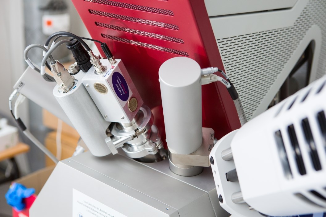
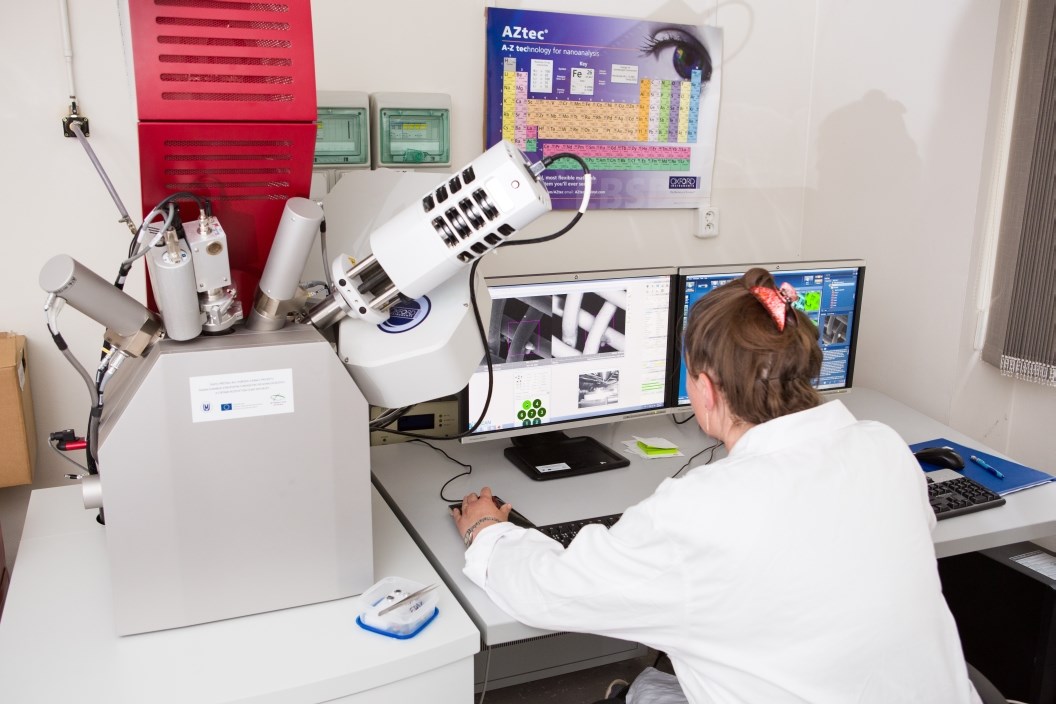
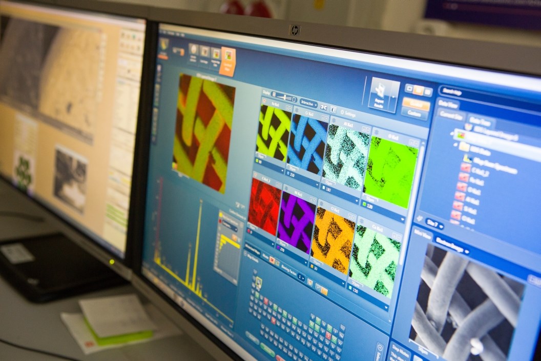
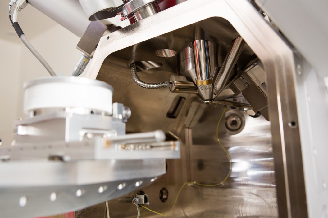
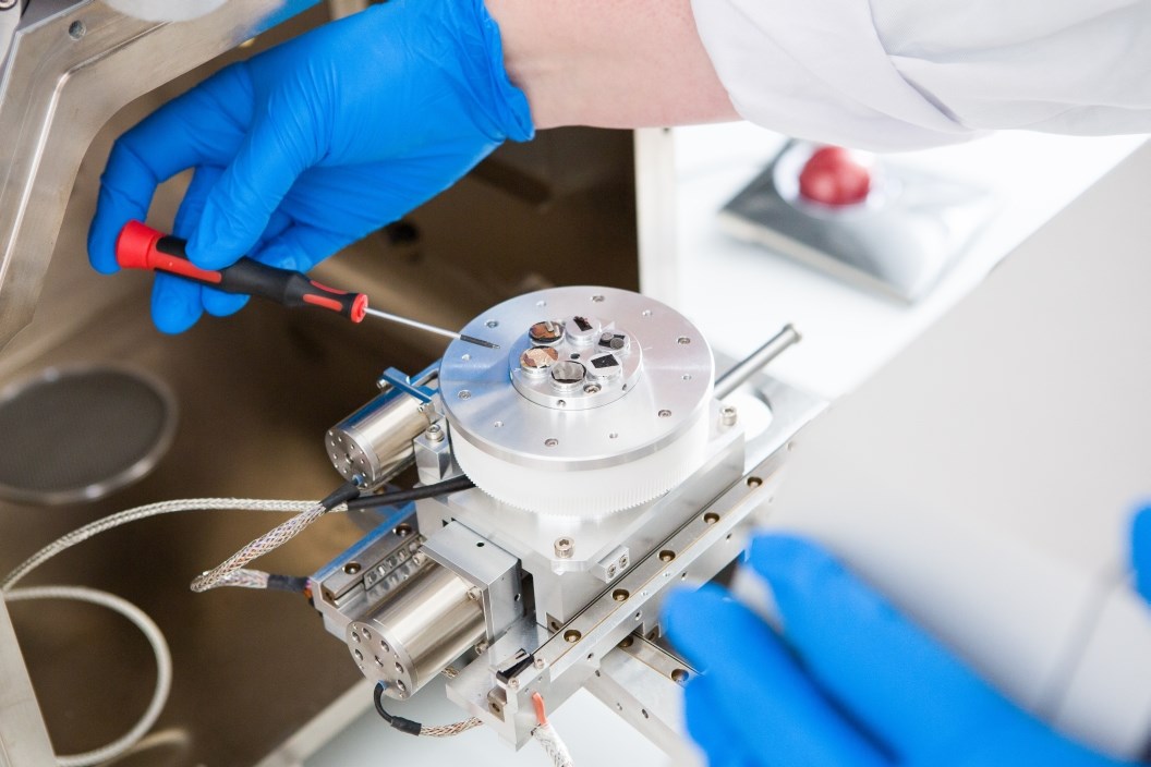
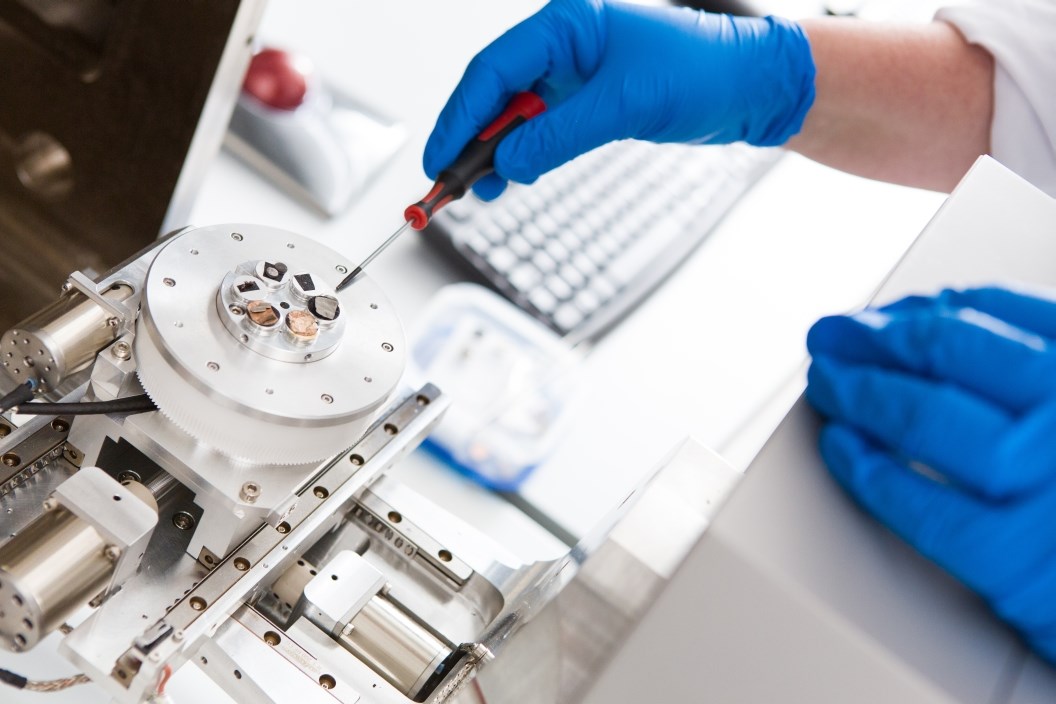
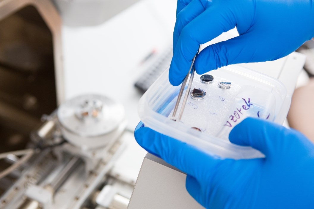
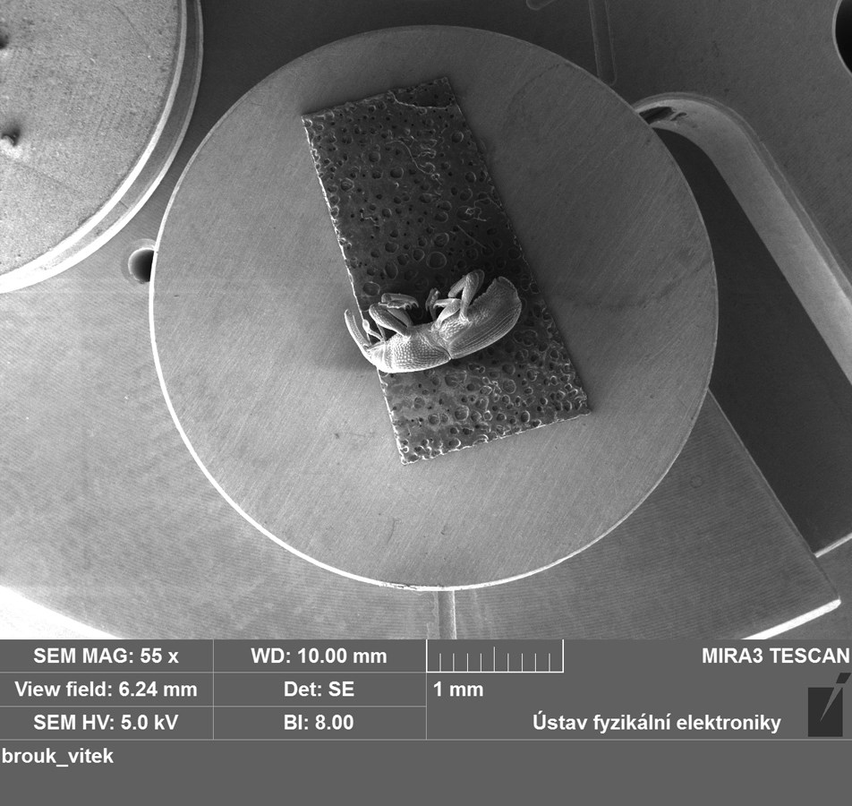
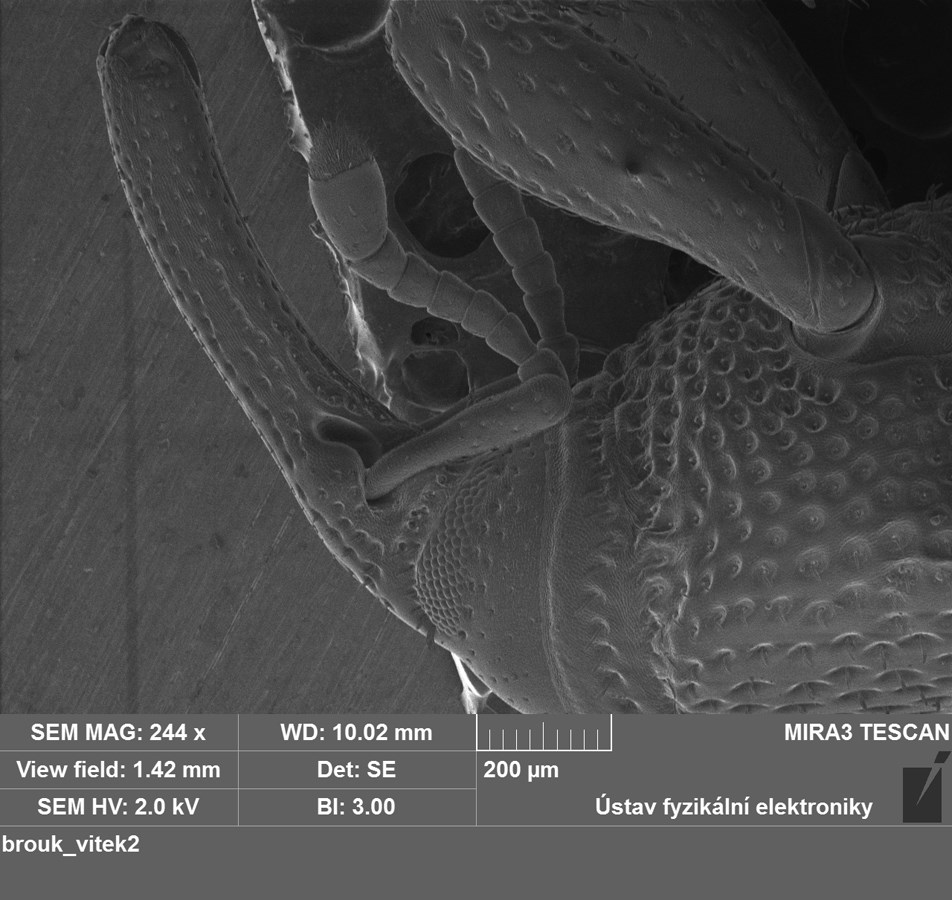
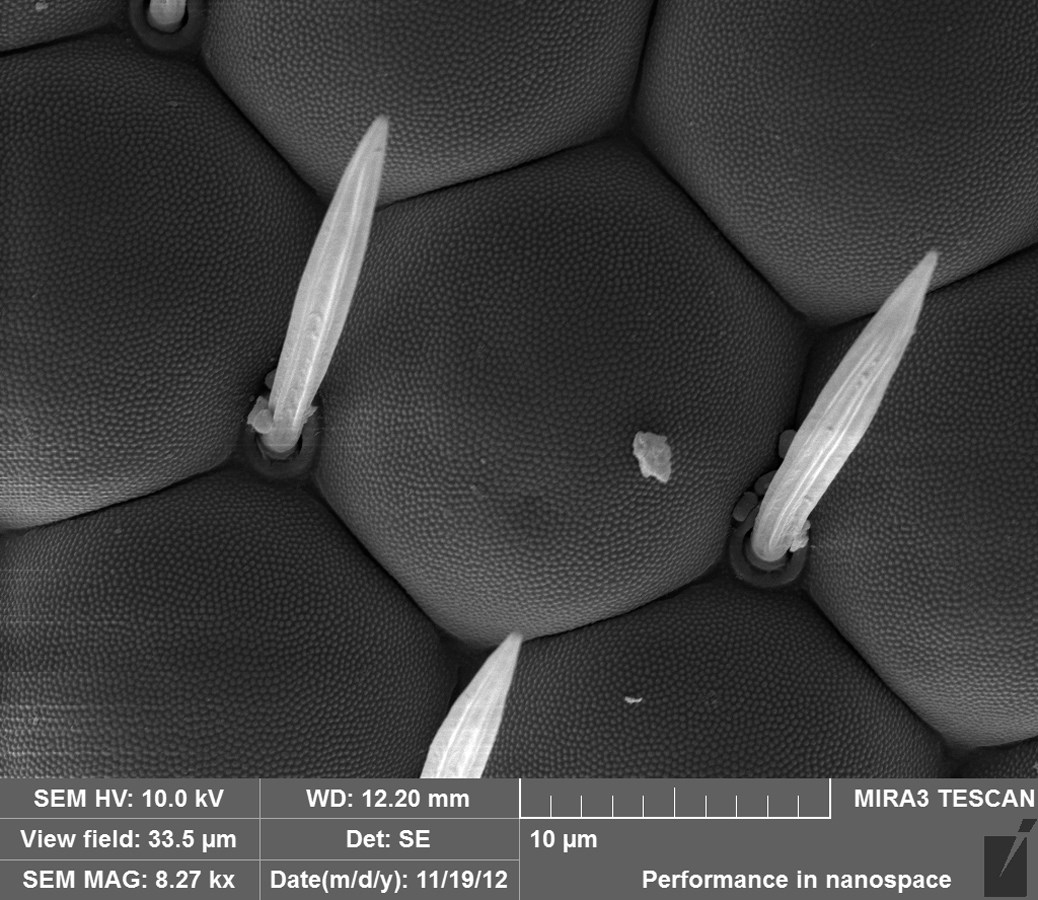
Scanning electron microscope – SEM
Scanning electron microscope MIRA3 made by Tescan, Brno is fully PC controlled SEM equipped with a Schottky Field Emission electron gun designed for high vacuum or variable pressure operations.
SEM equipped SE (Secondary electrons) and BSE (Back-scattered electrons) detectors. Both detectors are, as well, located in the objective lens enabling work at very short working distances for high resolution.
Parameters:
- Maximal resolution: 1 nm by 30kV
- Magnification range: 2x - 1 000 000x
Accessories:
- EDX - Energy Dispersive X-ray Spectroscopy
- WDS - Wavelength Dispersive Spectroscopy
- EBIC – Electron Beam Induced Current
Extended low vacuum mode with chamber pressure up to 500 Pa for non-conducting specimens imaging.


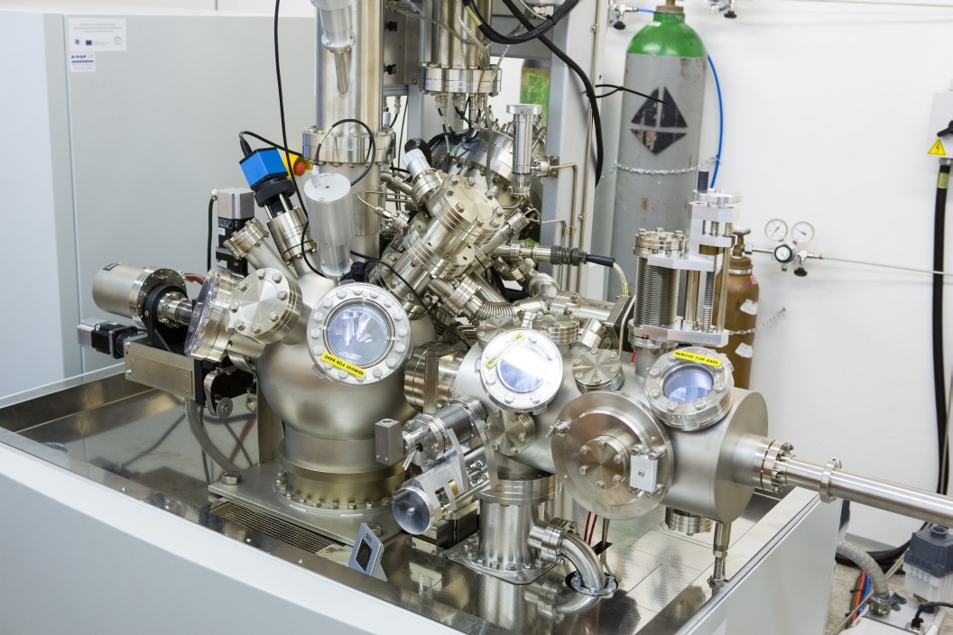
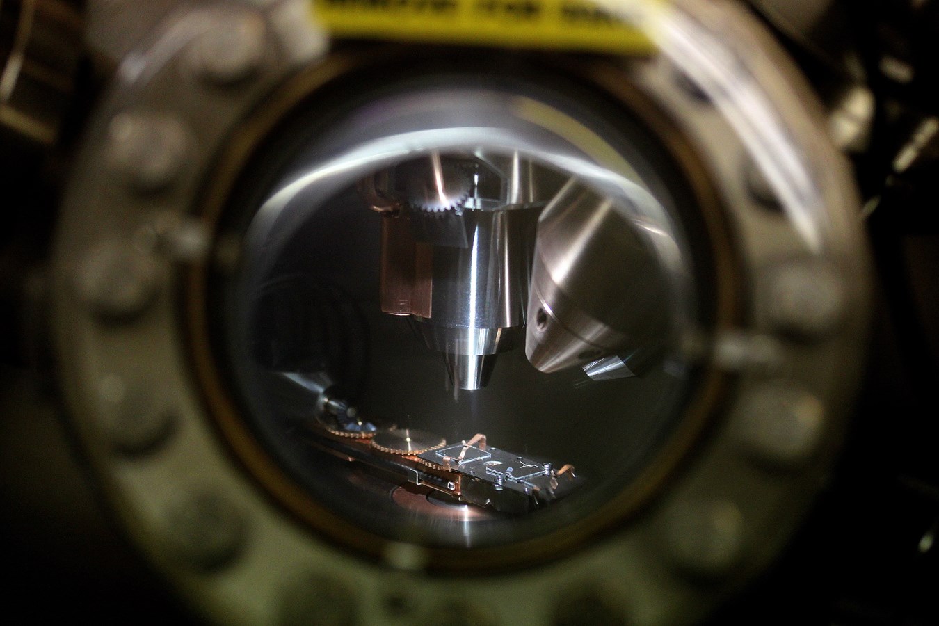
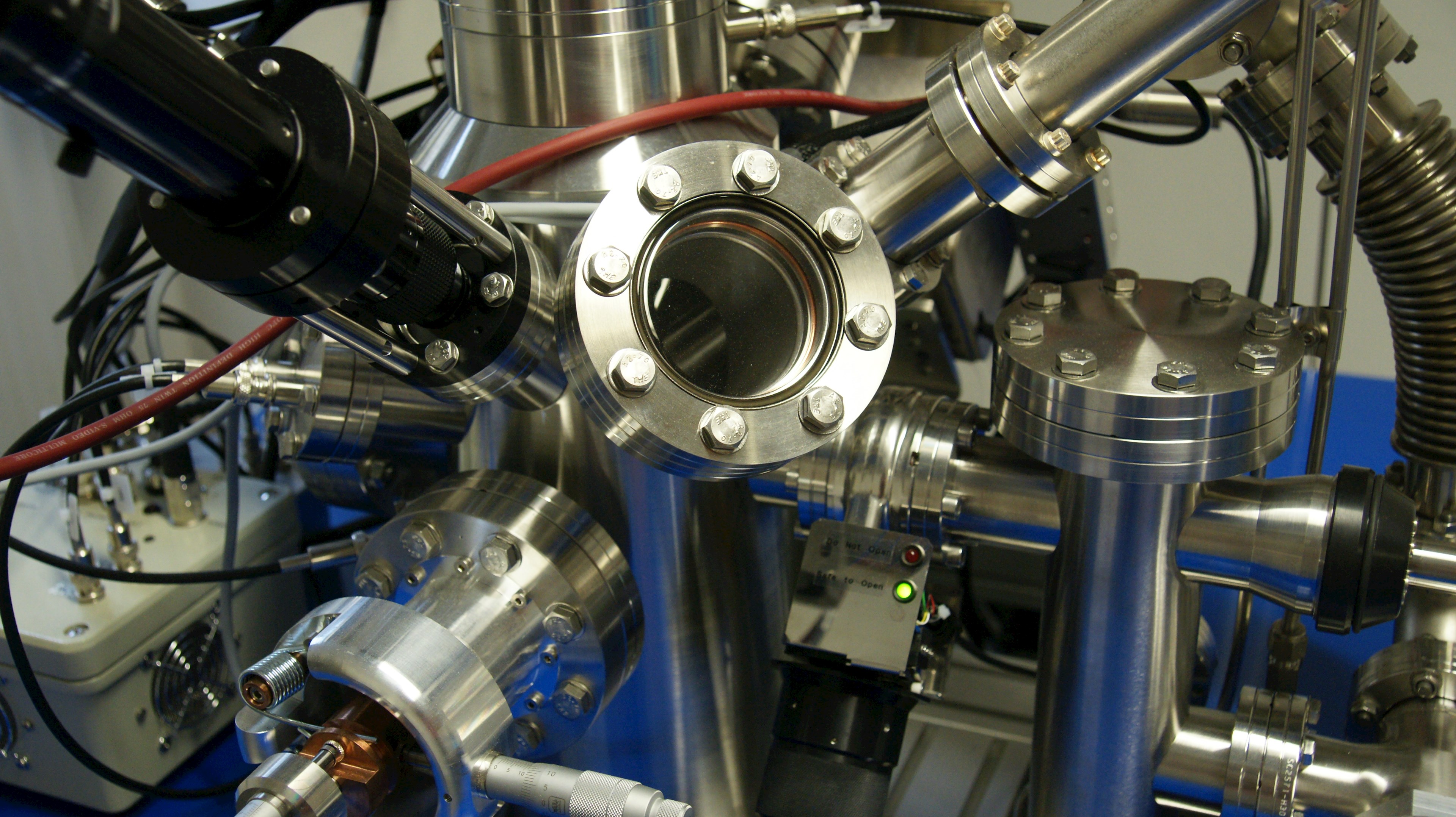
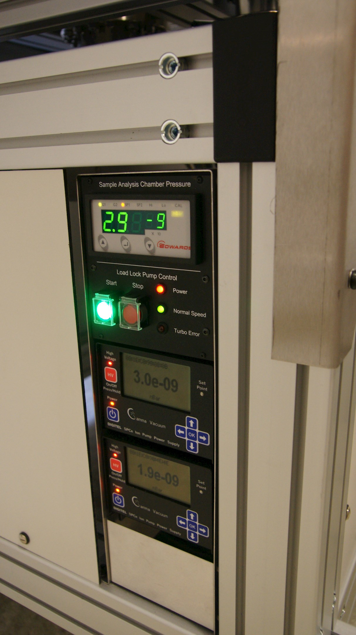
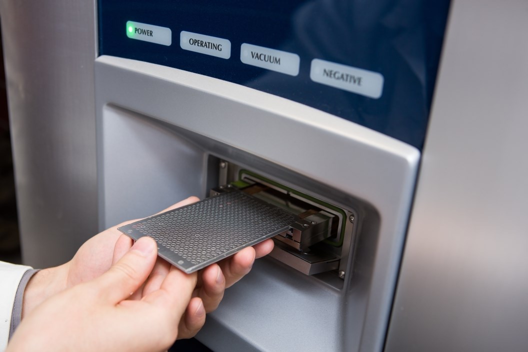
X-ray photoelectron spectroscopy – XPS
ESCALAB 250Xi (Thermo Scientific, UK) is extremely powerful XPS spectrometer coupling high sensitivity with high resolution quantitative imaging. This system is a multi-technique XPS for the analysis of the electronic characteristics and chemical composition of surfaces:
- Qualitative and quantitative detection of all elements (except for H and He)
- Information about spatial and depth distribution of the elements
- Chemical state analysis (including bonding and oxidation state)
- Determination of sorption capabilities/reactions (adsorption, ion-exchange, etc.)
Key Features:
- Photoelectron Spectroscopy
- Energy Resolution FWHM ≤ 0.45 eV of the Ag 3d5/2 peak
- Spatial Resolution ≤ 20 µm
- 2D Imaging/Mapping
- Spatial Resolution < 3 µm chemical imaging resolution
- Depth Profiling
- Angle Resolved XPS - destruction-free analysis, information depth ≤ 10 nm
- Destructive depth profiling by an ion etching, information depth ~ 1µm
- Small Area XPS - Small feature analysis from 20 to 900 µm
- Ultraviolet Photoelectron Spectroscopy
- Reflection Electron Energy Loss Spectroscopy
- Ion Scattering Spectroscopy
Applications:
- Polymers, Glasses, Ceramics
- Semiconductors
- Magnetic and dielectric materials
- Nanomaterials
- Catalysis
- Corrosion
- Biomedicine/Biotechnology
- Industry (Aerospace, Automotive, Pharmaceutical, Telecommunications, etc.)


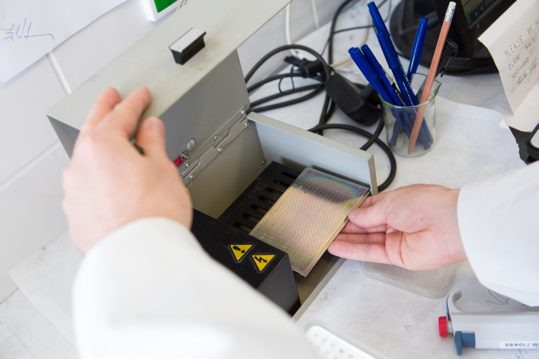
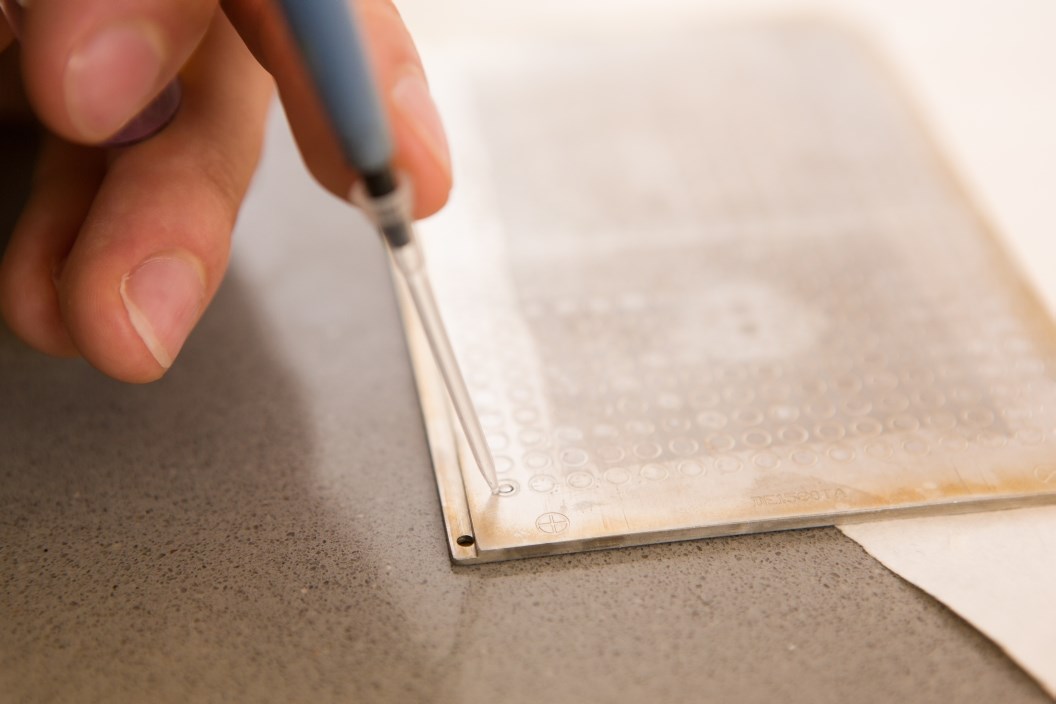
Secondary ion mass spectrometry – SIMS
SurfaceSeer –I is a highly sensitive surface analytical SIMS spectrometer offering detailed elemental and molecular information from the outer 1 to 2nm of materials. SurfaceSeer –I can work in a “static” mode with minimal damage to the sample surface (mass spectra and 2D spectral images) or in depth profile mode for in depth elemental and, in many cases, molecular analysis.
Parameters:
- Elemental and molecular information
- Isotopic analysis
- Very high surface sensitivity (1x10⁹atoms/cm2)
- Positive and Negative SIMS
- Conducting and insulating surfaces
- Mass resolution >3000 M/ΔM
- Mass range >1000 m/z
- Analytical spatial resolution to 0.5µm
- Sputter cleaning capability
Applications:
- Polymers, Glasses, Ceramics
- Semiconductors
- Magnetic and dielectric materials
- Nanomaterials
- Catalysis
- Corrosion
- Biomedicine/Biotechnology
- Industry (Aerospace, Automotive, Pharmaceutical, Telecommunications, etc.)


Atomic force microscope Ntegra Prima NT-MDT
Atomic force microscope Ntegra Prima NT-MDT is modular and it enable using various scanners from wide range of applications. The system has low thermal drift and excellent thermal stability, which play important role in case of applications where it is necessary to achieve high long-time position accuracy because of long-time experiments as well as nanomanipulation, electro-corrosion experiments, nanolitography etc.
Parameters:
- Scanning by probe and by sample, easy changing scanning modes
- Scan range: 100x100x12 mm
- XY sample positioning: 5x5 mm2
- Sensitivity better than 2 micrometres
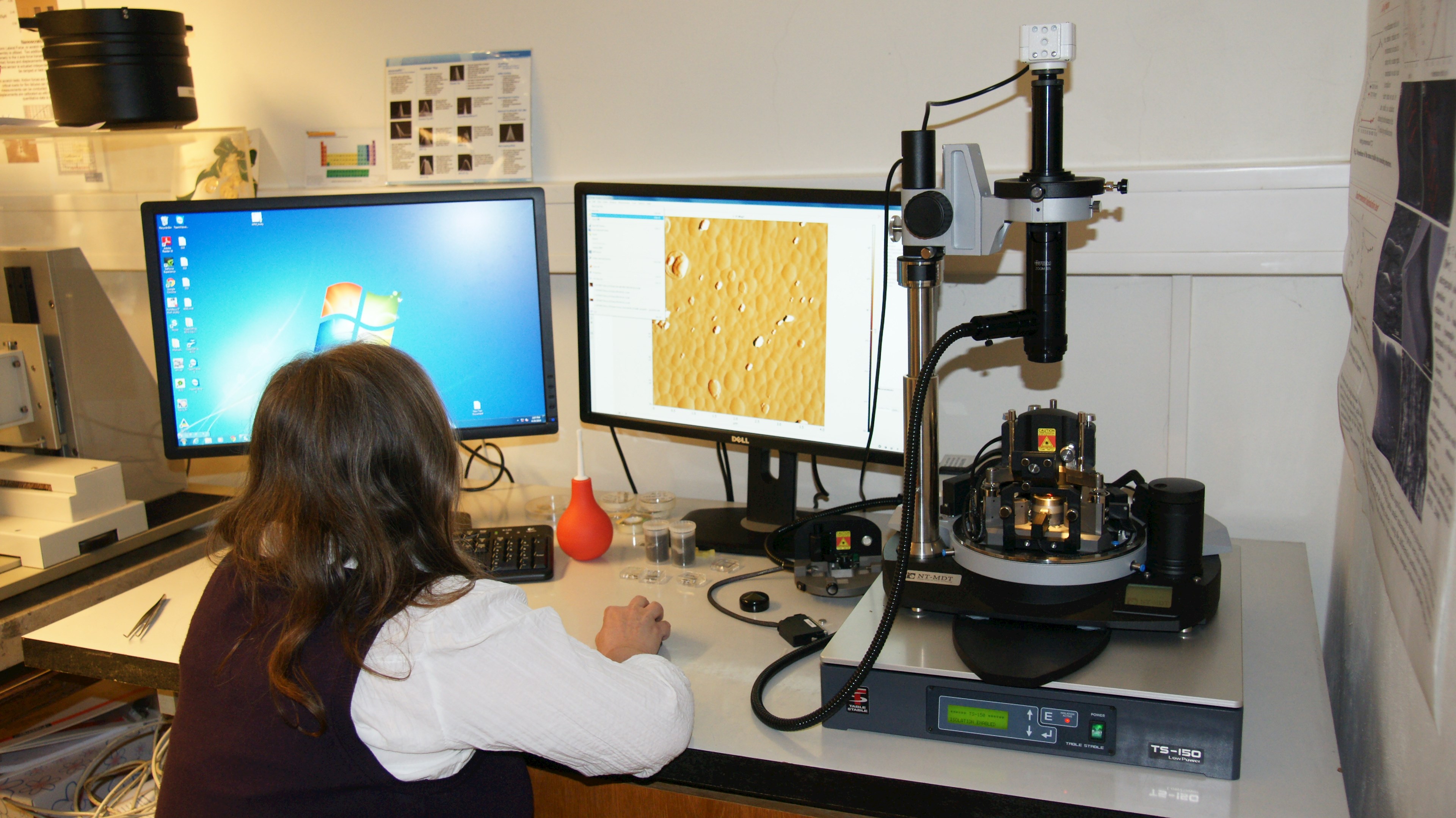

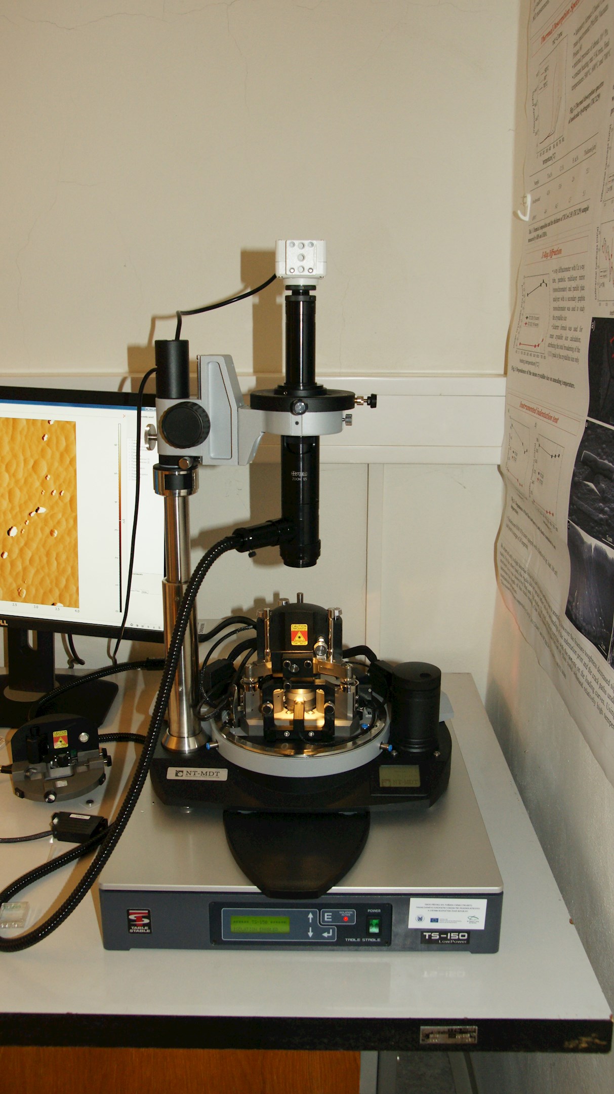
Testing modes:
- contact/non-contact mode
- lateral force mode
- phase contrast mode
- magnetic and electric
- force microscopy force modulation
- resonance spectroscopy
- kelvin probe
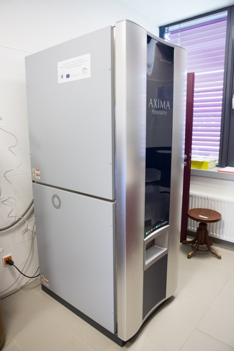
Matrix-assisted laser desorption/ionization – MALDI
AXIMA Resonance is a versatile MALDI TOF mass spectrometer employed in a broad range of applications. Its main advantages are low sample consumption, high resolution, high accuracy of the m/z and ability to isolate parent ions with isotopic resolution over a wide mass range from 100 to 20000 Daltons. The molecules are analysed in positive or negative ion modes.
Accessories:
- Variable repetition rate N2 laser (337 nm) for desorption of the sample.
- Quadruple ion trap allows the high-resolution selection of parent ions and highly controlled collision induced dissociation (CID) for high-sensitivity MSn acquisitions.
- TOF mass spectrometer in reflection mode promotes high resolution and high mass accuracy for all ions generated.
- Software solution for a wide range of applications enables manual or fully automated operation for few or many samples, as required.
Applications:
- Analysis of small molecules – organic and inorganic.
- Structural characterization and identification of synthetic polymers.
- Structural characterization and sequencing of biomolecules like peptides, proteins, etc.
- It can also be applied to follow purity of various materials, drugs, medicaments, to analyse polymers and also thin or nano-layers. Characterization of purity of glass, silicon, metals etc. surfaces is possible if the thickness of sample is below 0.5 mm.


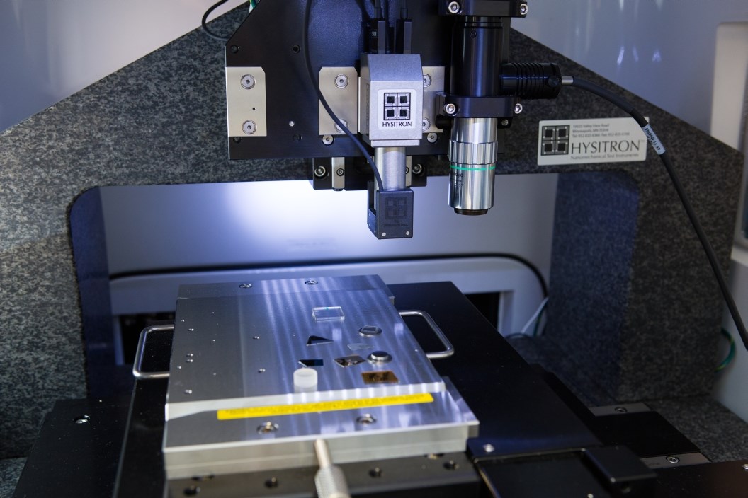
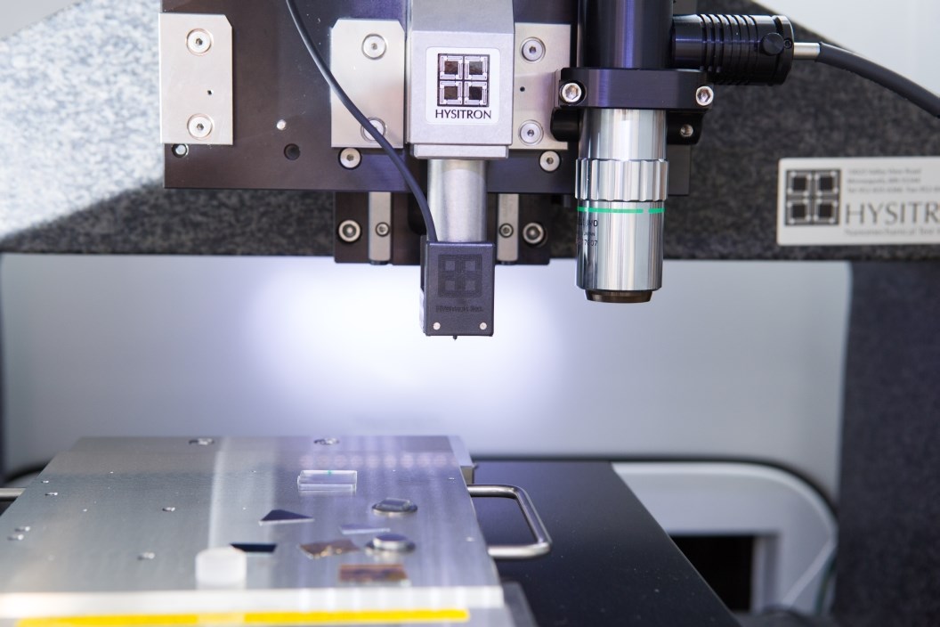
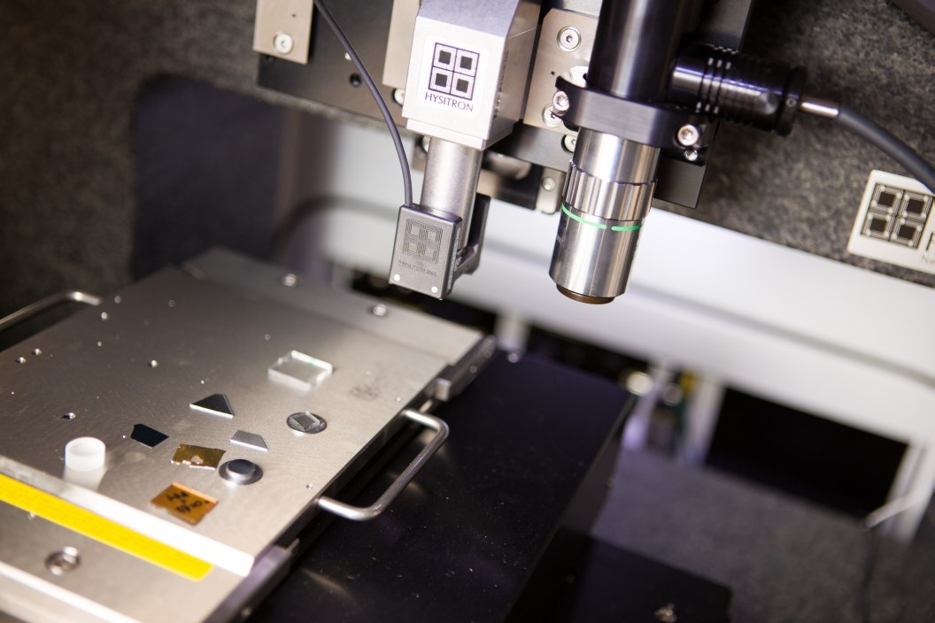
Nanoindenter Hysitron
The Hysitron TI 950 TriboIndenter is the next generation nanomechanical test instrument providing industry-leading sensitivity and unprecedented performance. The TI 950 has been developed as an automated, high throughput instrument to support the numerous nanomechanical characterization techniques developed by Hysitron.
Testing modes:
- Quasistatic nanoindentation – Measure Young’s modulus, hardness, fracture toughness and other mechanical properties via nanoindentation
- Scratch testing – Quantify scratch resistance, critical delamination forces, and friction coefficients with simultaneous normal and lateral force and displacement monitoring
- Top-down optics – High- resolution, color CCD camera for individual structure identification and coarse test positioning
- SPM imaging – In-situ imaging using the indenter tip provides nanometer precision test positioning and surface
- topography information
- ScanningWear™ – Observe and quantify wear volumes and wear rates using the in-situ imaging capability
- Feedback control – Operate in closed loop load or displacement control for superior nanoindentation and creep

Transducer Specifications:
- Load:
- Resolution: <1 nN
- Noise Floor: <30 nN
- Imaging Contact Force: ≤70 nN
- Displacement:
- Resolution: <0.02 nm
- Noise Floor: <0.2 nm
- Drift: <0.05 nm/sec
Stage Specifications:
X and Y stages:
- Travel: 250 mm × 150 mm
- Encoder Resolution: 500 nm
Applications:
- Testing of mechanical and tribological properties of thin films, coatings and plasma treated surfaces from nano- to microscale
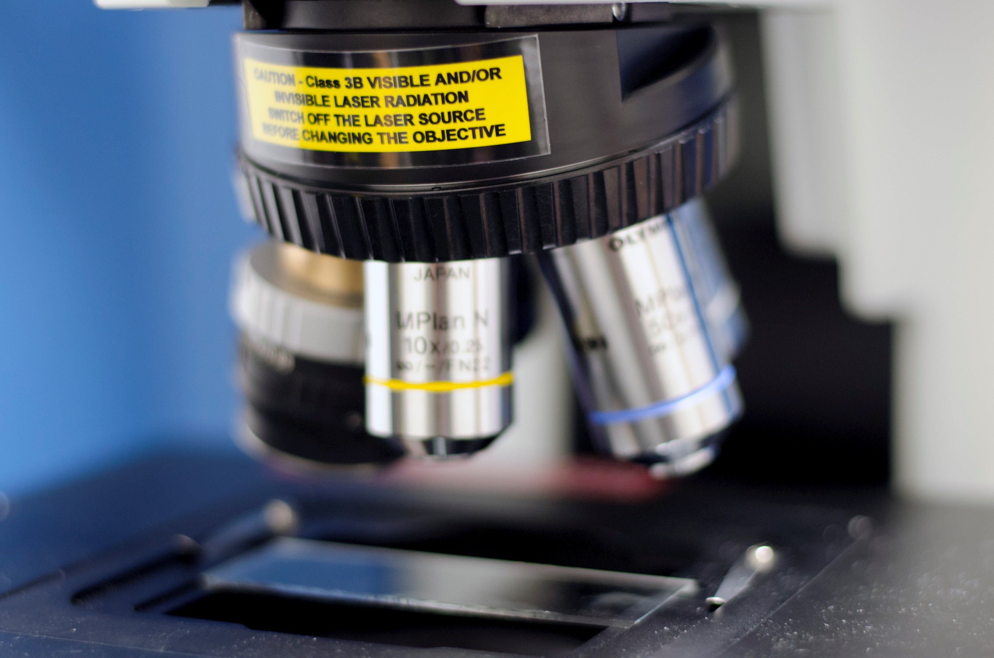
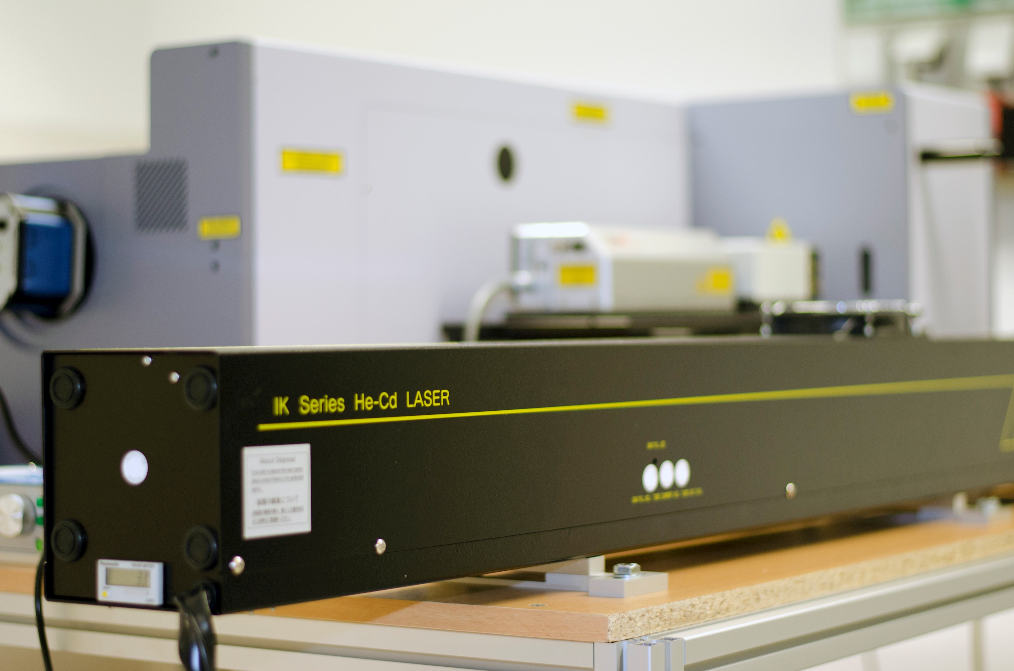
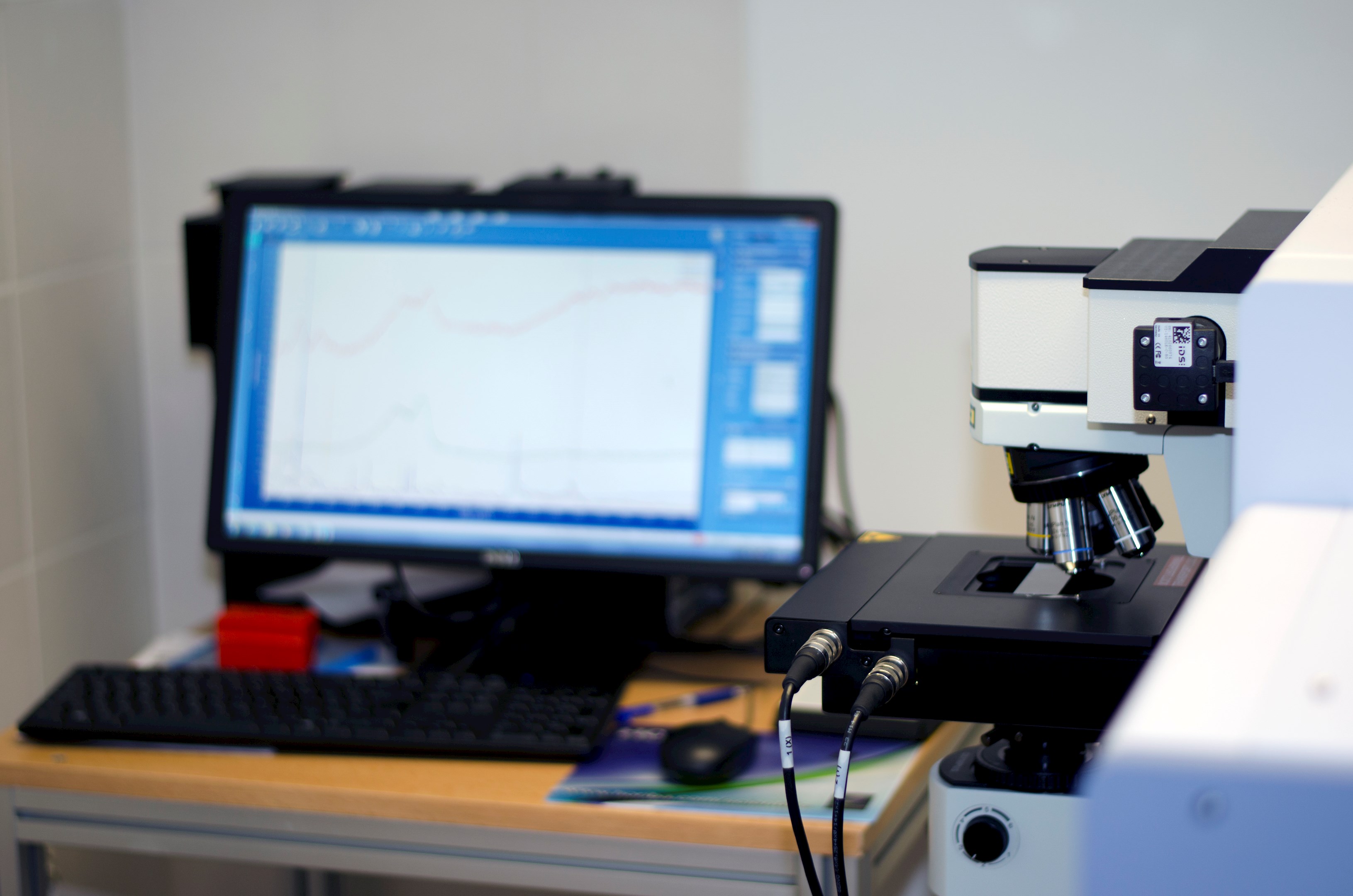
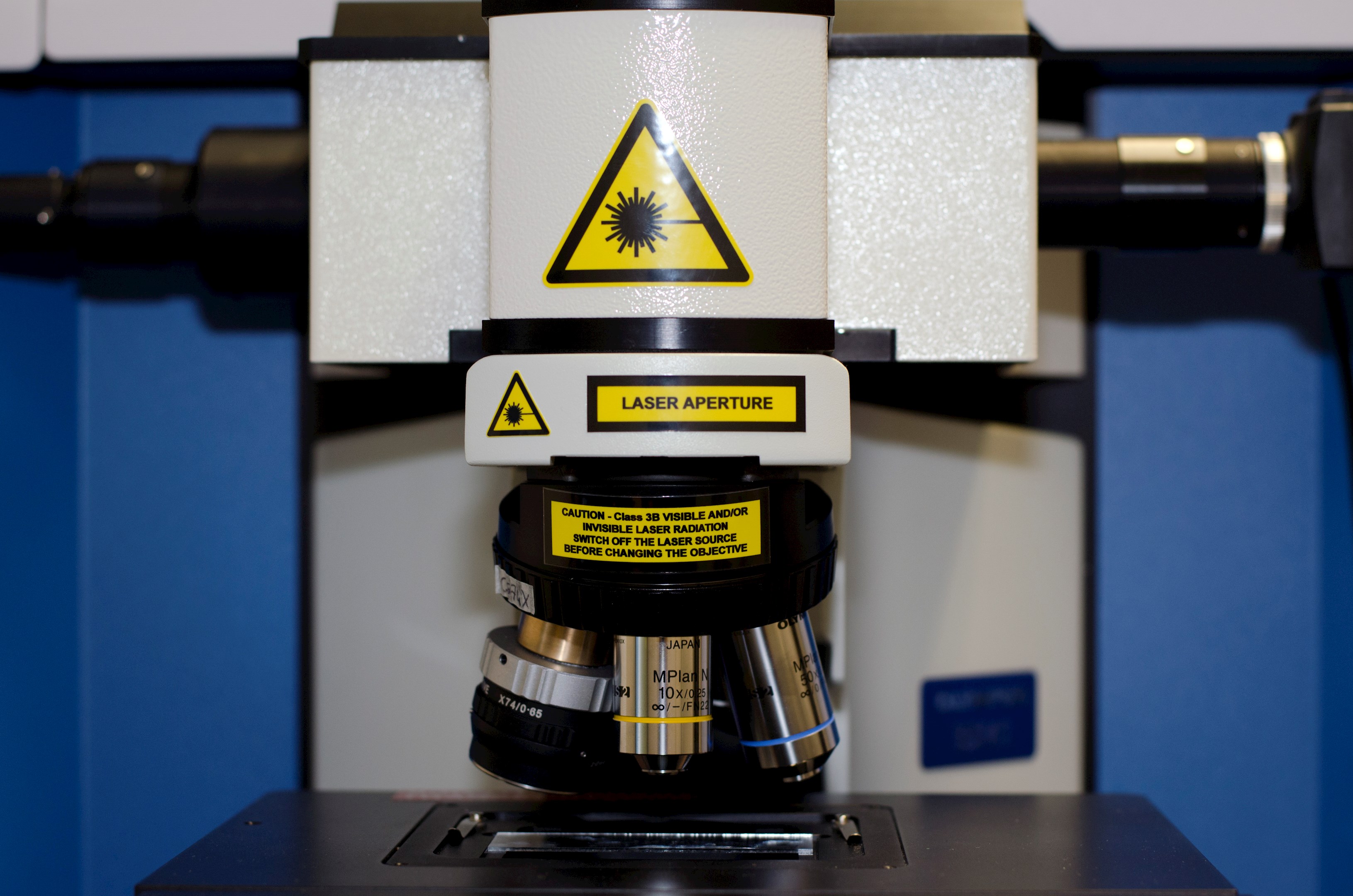
Raman microspectrometer HORIBA
LabRAM HR Evolution system by HORIBA is ideally suited for measurement of vibrational, rotational and overall low energy molecule modes for chemical analysis in both micro and macro scale. Thanks to wide measurement scale of 10 – 2200 cm-1 and a long focusing distance, it is possible to perform measurements with high spectral resolution from ultraviolet to visible to infrared region. Thanks to the high resolution and low noise measurements, it is possible to get accurate information about the crystallinity, polymorphism and overall state of the surface molecules. In addition to point measurements, it is possible to perform 2D and 3D mapping of the sample using optically coupled confocal microscope and fully motorized sample stage.
Parameters:
High flexibility of Raman analysis is provided by three laser sources - HeCd 325 nm, semiconductor 532 nm laser and a second semiconductor laser at 785 nm. The detector is fitted by a 1024 x 25s pixel CCD with very high spectral resolution of 0.5 cm-1/pixel for 325 nm laser up to 0.2 cm-1/pixel for 785 nm laser. The focusing distance of the spectrometer is 800 mm. The laser is optically coupled with a confocal microscope equipped with 10x, 50x and 100x objectives as well as fully achromatic (cassegrain) 74x objective. In addition the sample stage is fully motorized in X,Y axes (75 x 50 mm with the step of 0.1 micrometers) as well as Z axis (step of 0.01 micrometers) and therefore high spectral and spatial definition sample surface mapping is possible.
Applications:
- Raman analysis of samples with high spectral and spatial definition 2D and 3D mapping possible
- Wide spectral range measurements NIR-VIS-UV 10 – 2200 cm-1 for wide range of samples

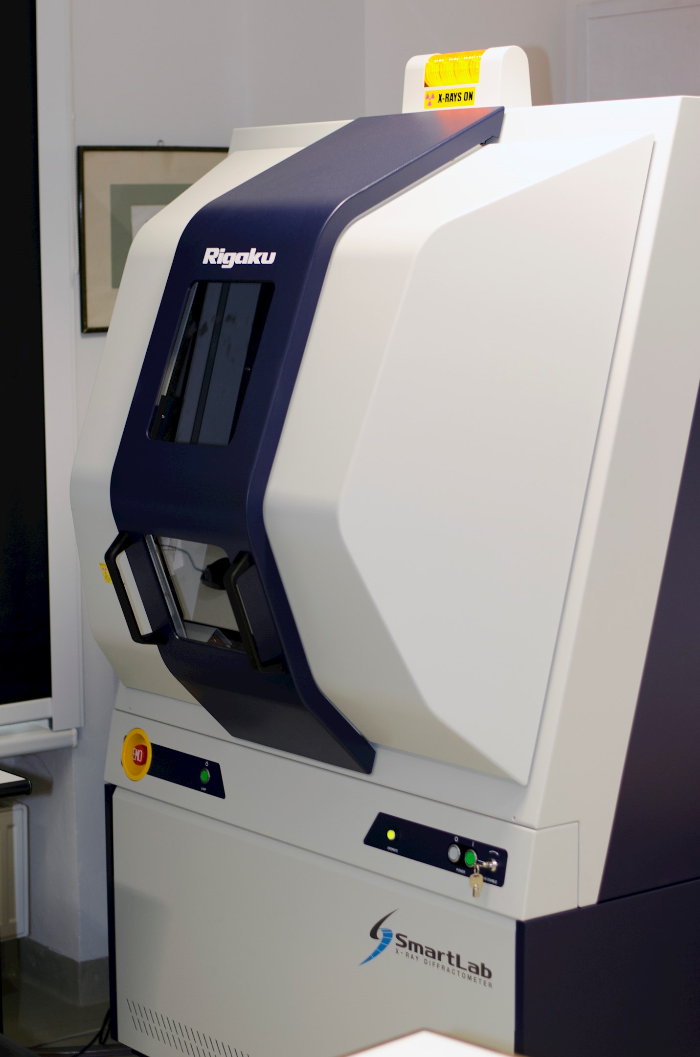
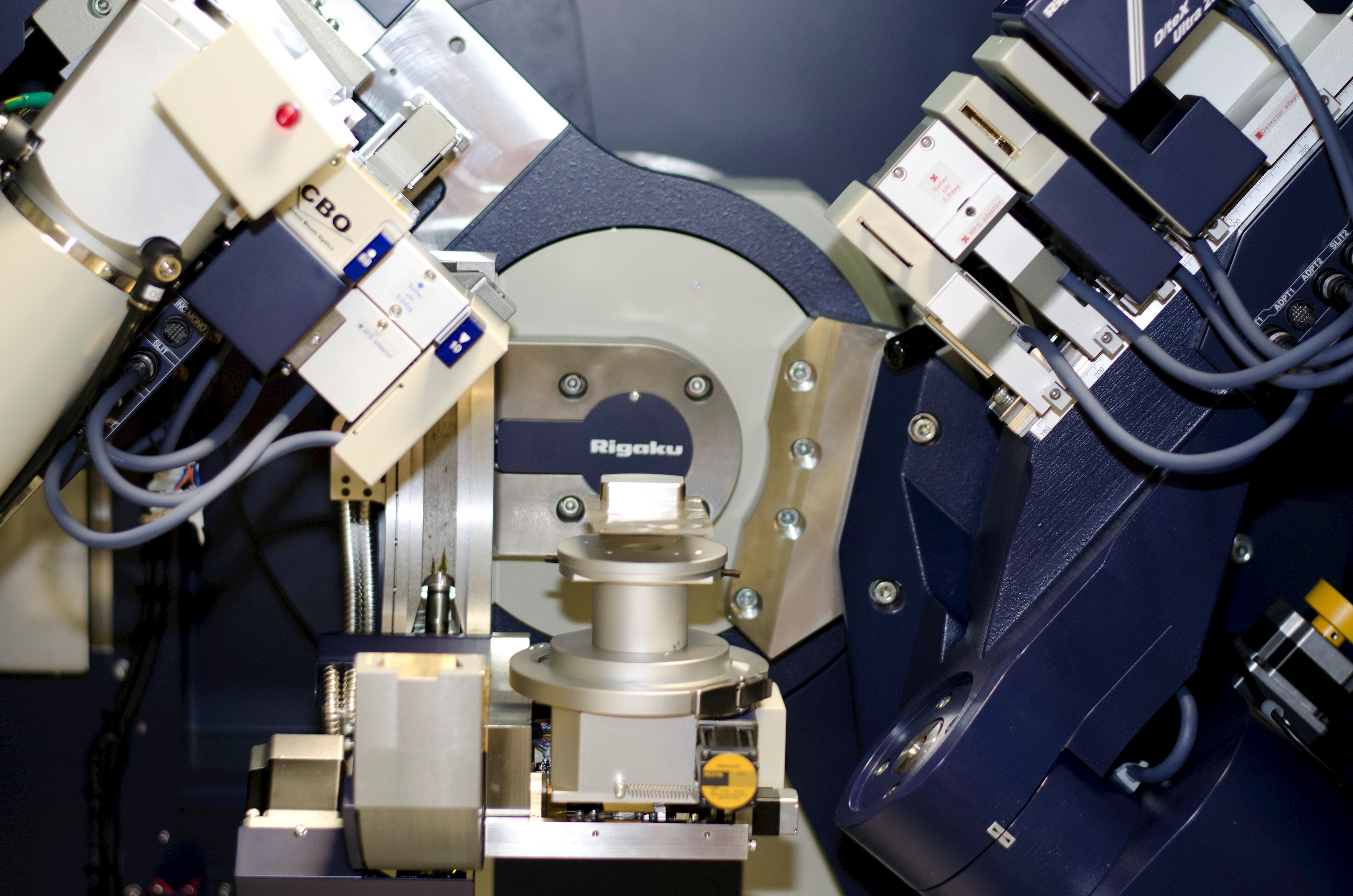
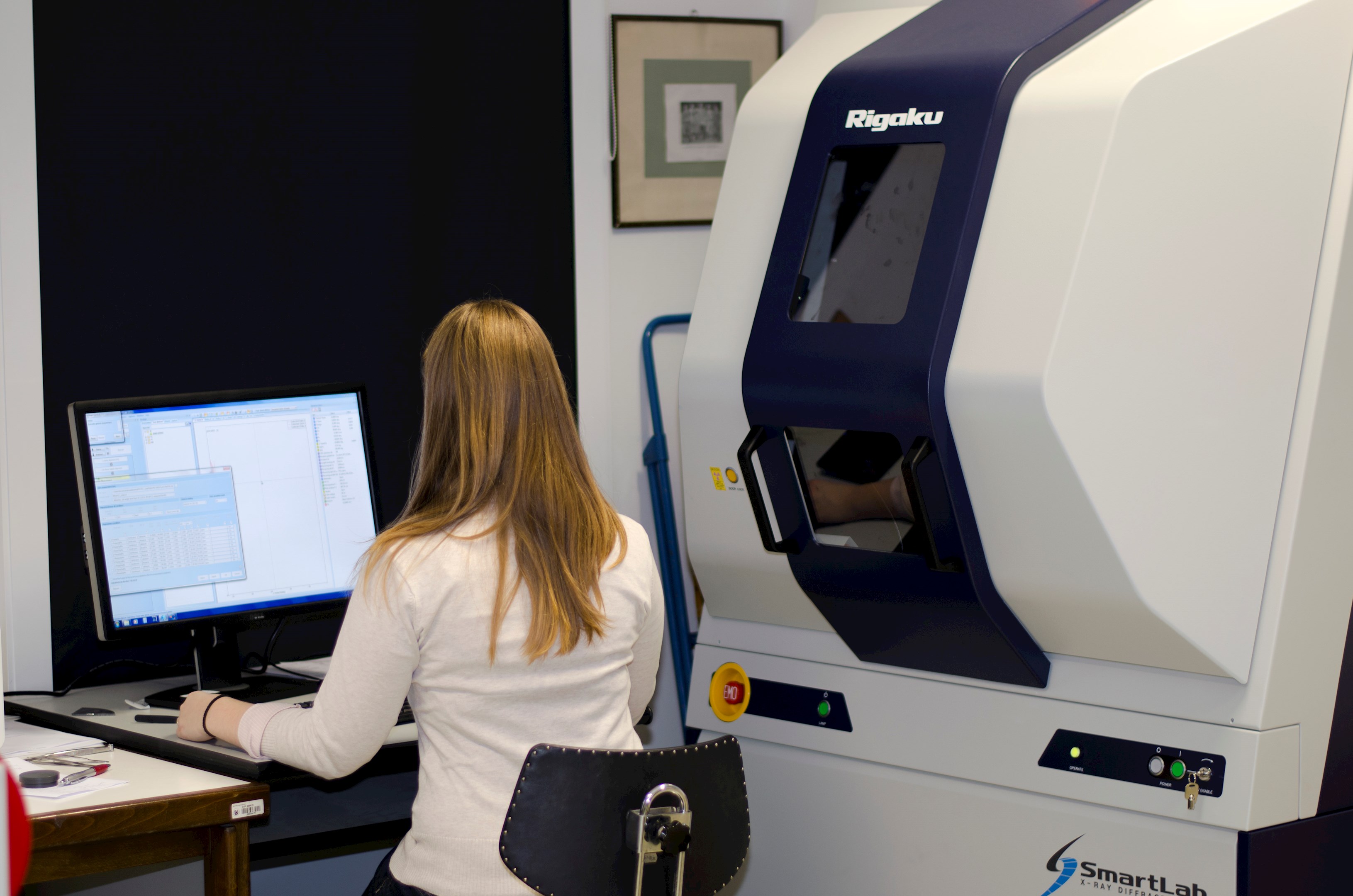
X-Ray difractometer
X-Ray Difractometer SmartLab Type F from experienced Japanese manufacturer Rigaku presents one of the most powerful and versatile serially produced machines up-to-date. It is possible to measure samples in the form of thin films, multi-layers, as well as powders, nano-particles and bulk. Measurement of single diffraction patterns as well as sample mapping and measurement of small angle X-ray scattering (SAXS) is possible. The measurement can be performed in wide angles, thus enabling us to measure a wide variety of crystalline samples. It is possible to perform qualitative and quantitative phase analysis, stress analysis and measure the texture and pole figures for samples up to size of 6”.
Parameters:
The device is equipped with a sealed X-ray source with copper anode and vertical theta-theta goniometer with horizontal sample site with independent source and detector movement. The smallest goniometer step is 0,0001°, which enables us to perform high definition measurements. The goniometer movement is limited to a wide arc of -3° - 160° (2 theta). The sample can be tilted from -5° to 95°. In-plane measurements with horizontally attached sample can be performed using in-plane detector movement in the range of -3° - 120°. 1D detector in Bragg-Bretano configuration as well as 0D detector in parallel beam configuration can be used for the measurement. This versatile configuration enables us to measure both out-of-plane and in-plane diffractions. SAXS and reflectivity measurement adaptors are also available.
Applications:
- Structural and phase analysis of crystalline samples
- Low and high resolution measurements available
- Samples in the form of powders, nano-particles, mono- and multi-layer as well as bulk samples can be measured
- Sample size from several millimetres to 6“ wafers


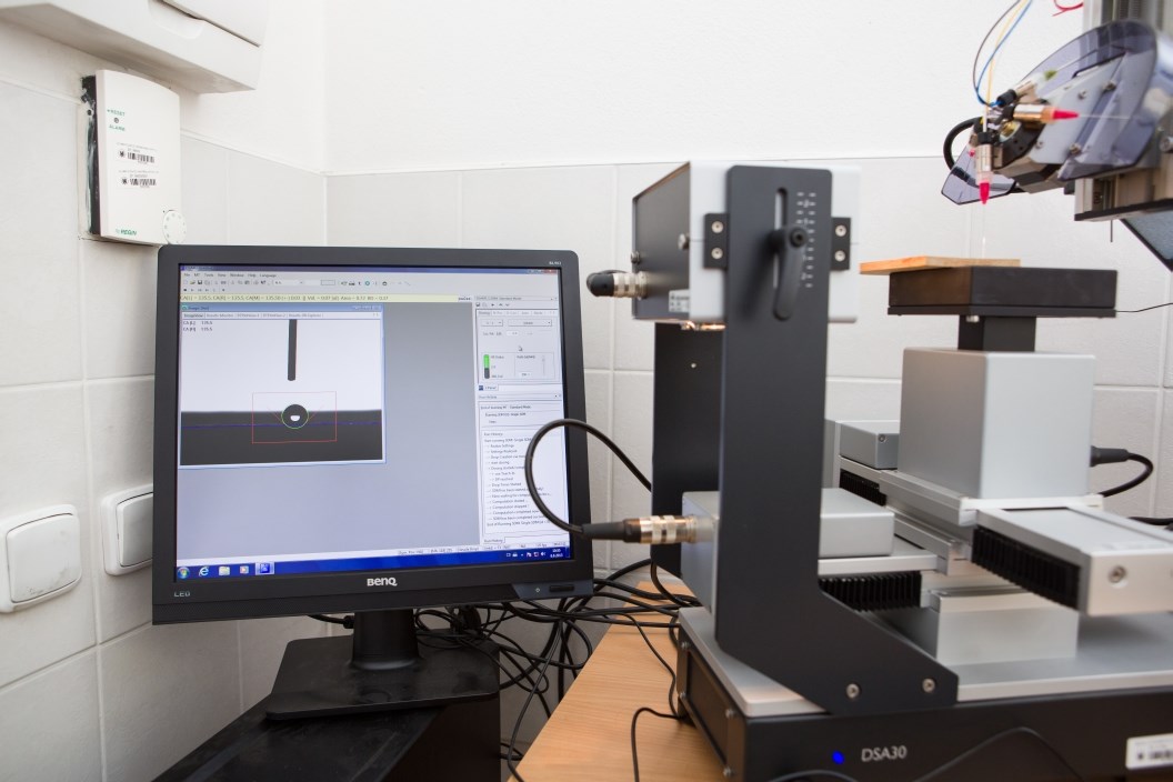
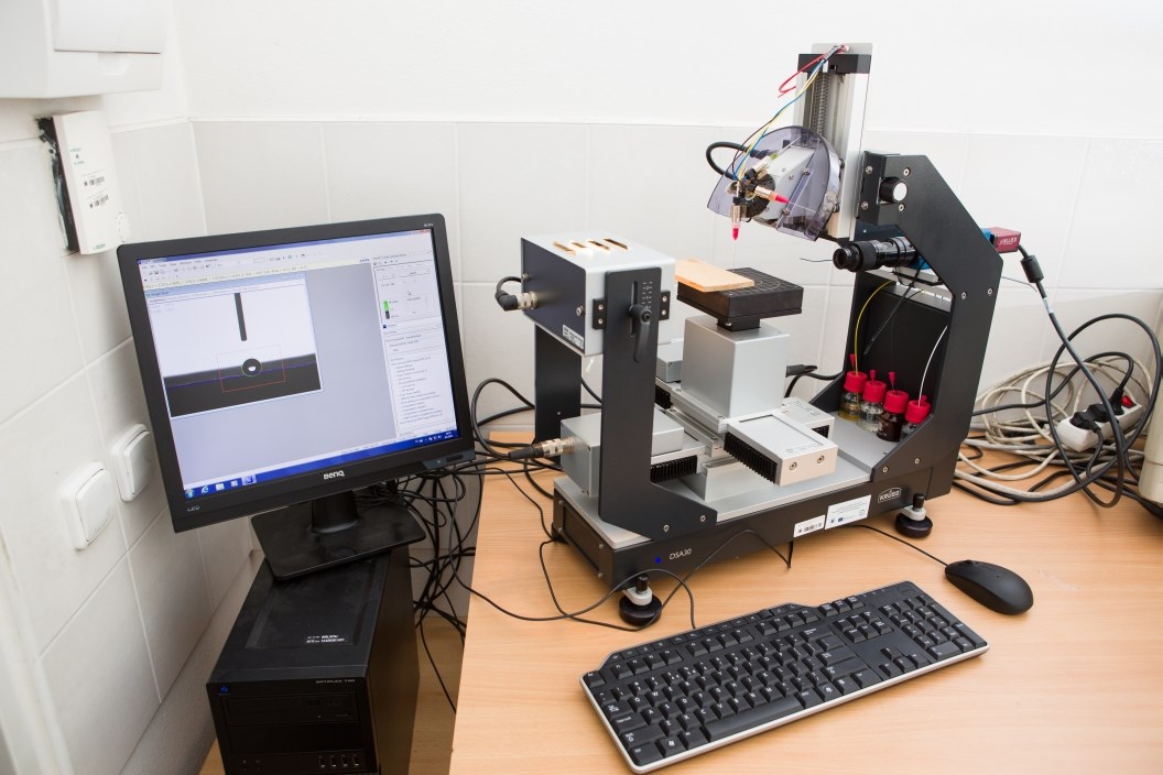
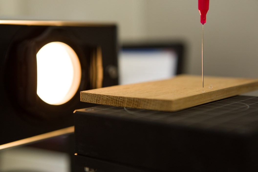
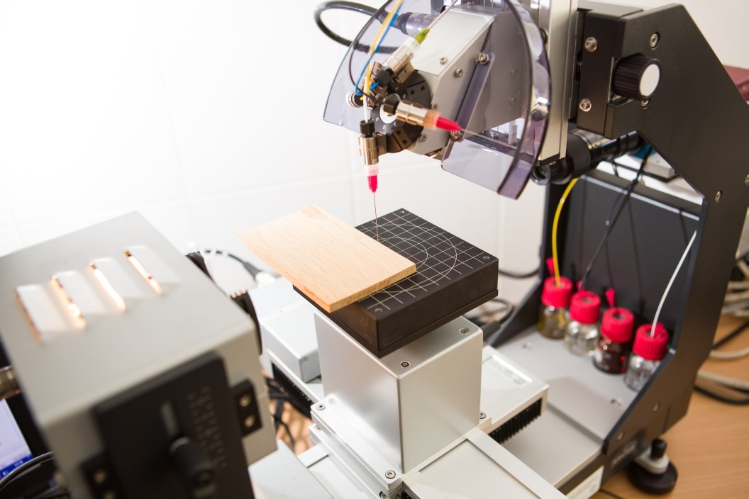
Dynamic Contact Angle System
DSA 30 (Krüss, Germany) software controlled system for quick measuring of static and dynamic contact angles. The contact angle study can provide important information about surface properties including the free surface energy.
Parameters:
- CCD camera, 61 fps (780 × 580 px) or 311 fps (780 × 60 px)
- Axis: Software controlled x, y, z axes
- Contact angle range: 1 - 180°, Contact angle resolution: 0.1°
- Surface energy range: 1×10⁻² – 1000 mN/m (mJ/m2), Surface energy resolution: 0.01 mN/m (mJ/m2)
- Video sequences, automatic triggering of measurements
Software:
- 6 different methods of drop shape analysis
- Automatic baseline detection
- Autodrop delivery
- Pendant drop method
- Surface and interfacial tension of liquids
Applications:
- Various surfaces: Si-wafers, glass, polymers, etc.

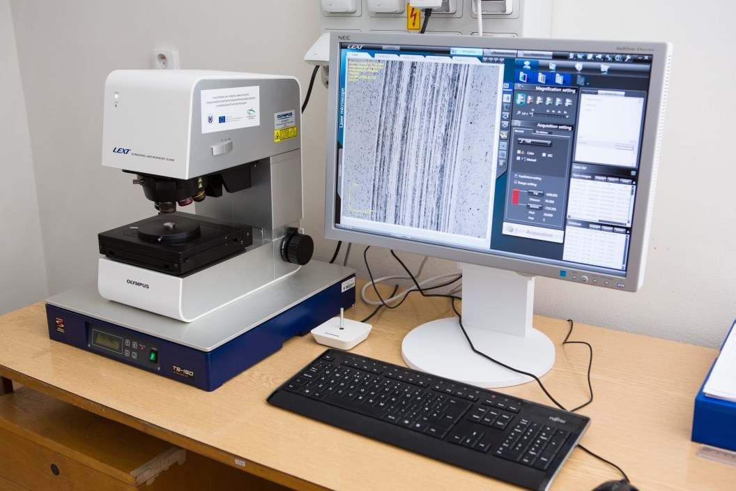
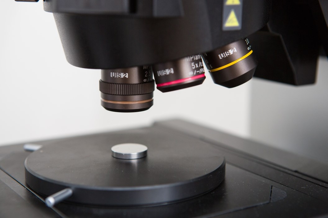
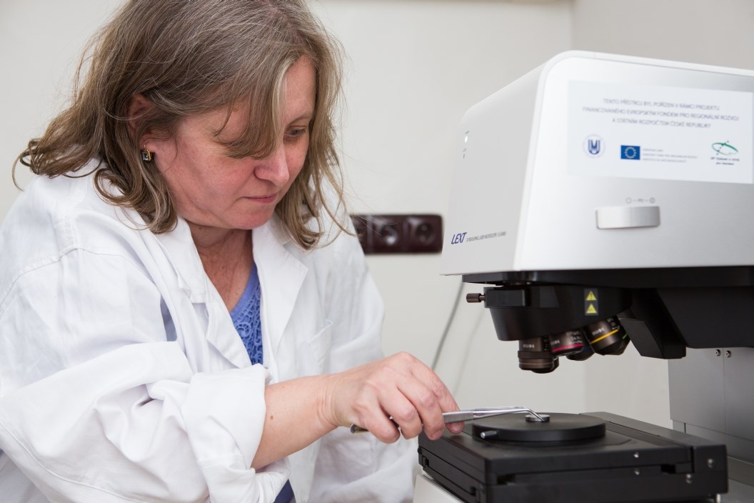
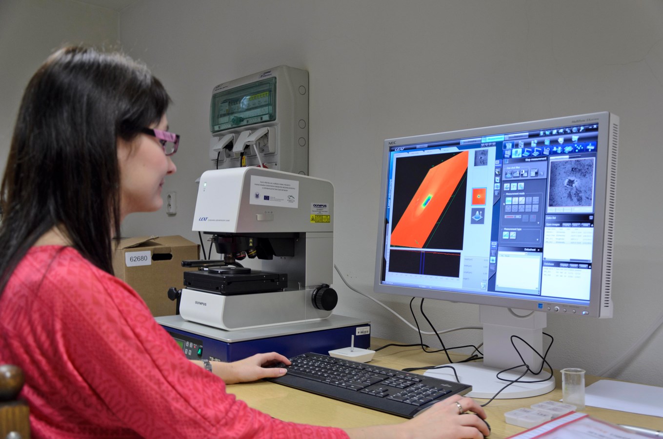
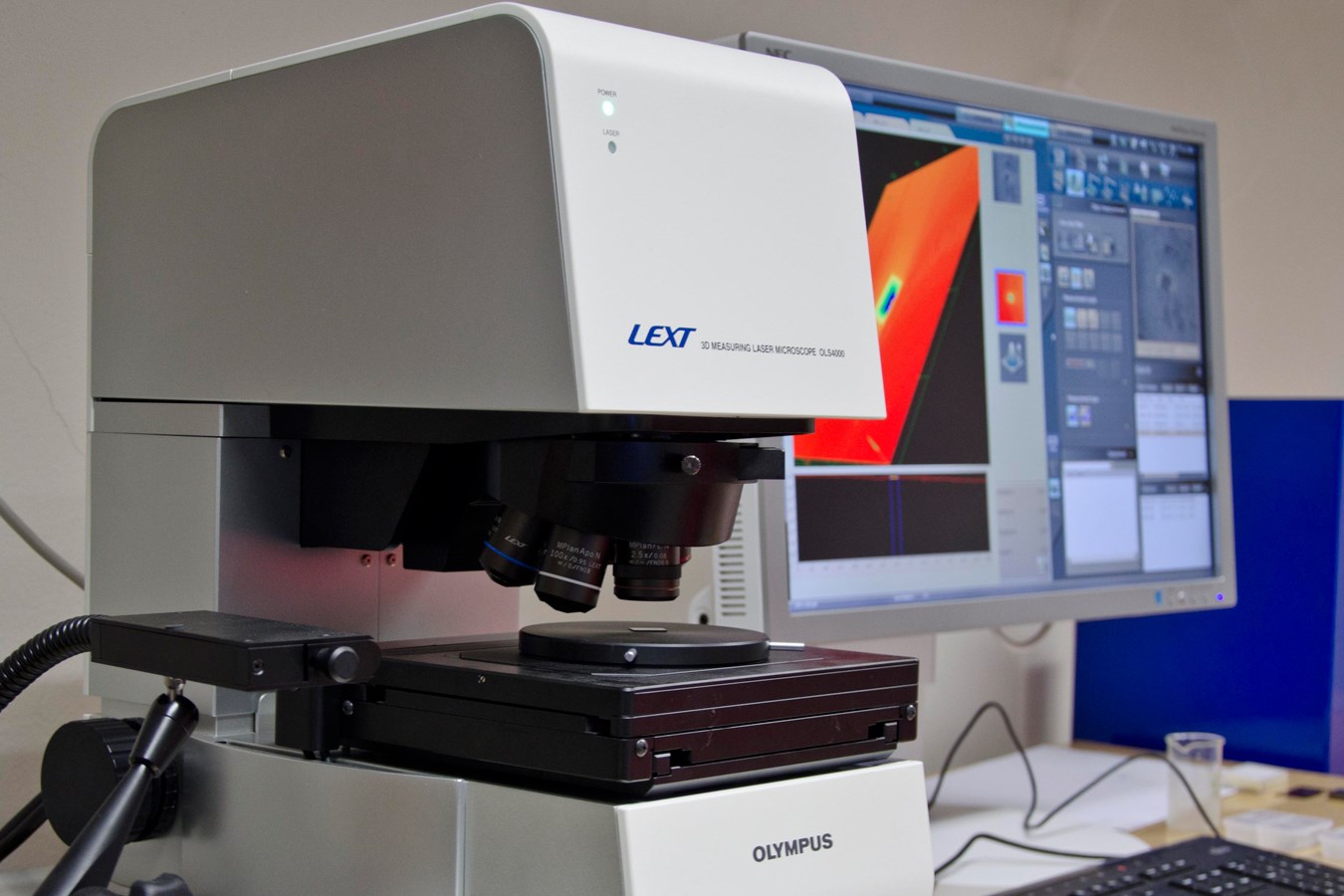
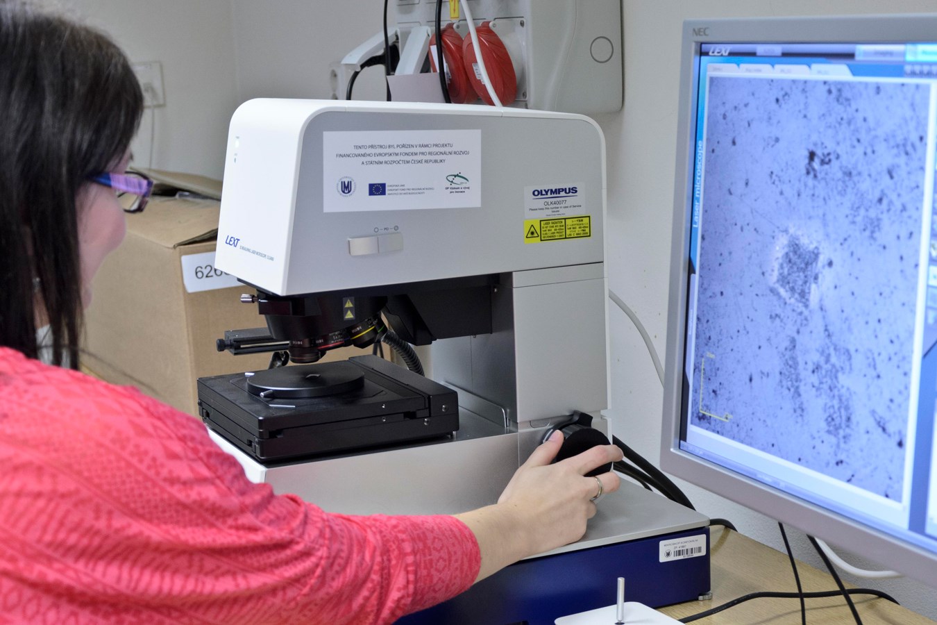
Confocal laser microscopy – CLM
The LEXT OLS4000 3D Laser Measuring Microscope is designed for nanometer level imaging, 3D measurement and roughness measurement.
Parameters:
- Optical system: UIS2 Optical System (Infinity-corrected)
- Total magnification: 108x - 17280x
- Field of view: 2560x2560 - 16x16 µm
- Microscope frame
- Observation method: BF/DIC/Laser/Laser Confocal DIC
- Laser: 405 nm Semiconductor Laser
- White light: White LED
- Focus: Z Stage Stroke: 100 mm, Maximum Height of Specimen: 100 mm
- Z revolving nosepiece: Stroke 10 mm, Resolution 0.01 µm, Repeatability σn-1=0.012 µm
- Objective lens: 5x, 10x, 20x, 50x, 100x
- Optical zoom: 1x - 8x
- Stage: Motorized Stage 100x100 mm
- Dimensions: 276(W)x358(D)x405(H) mm
- Weight: 32 kg (Main Unit)
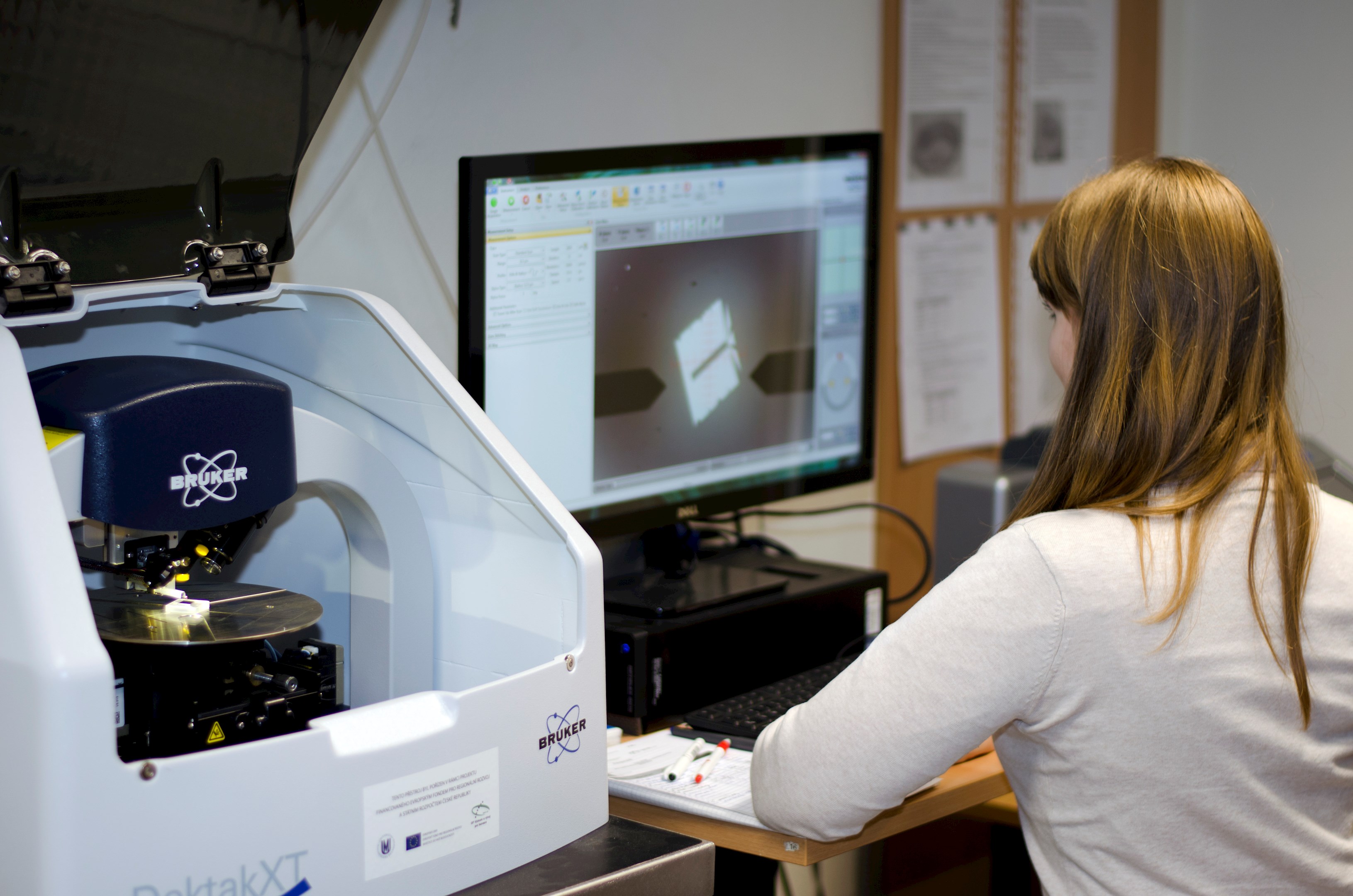
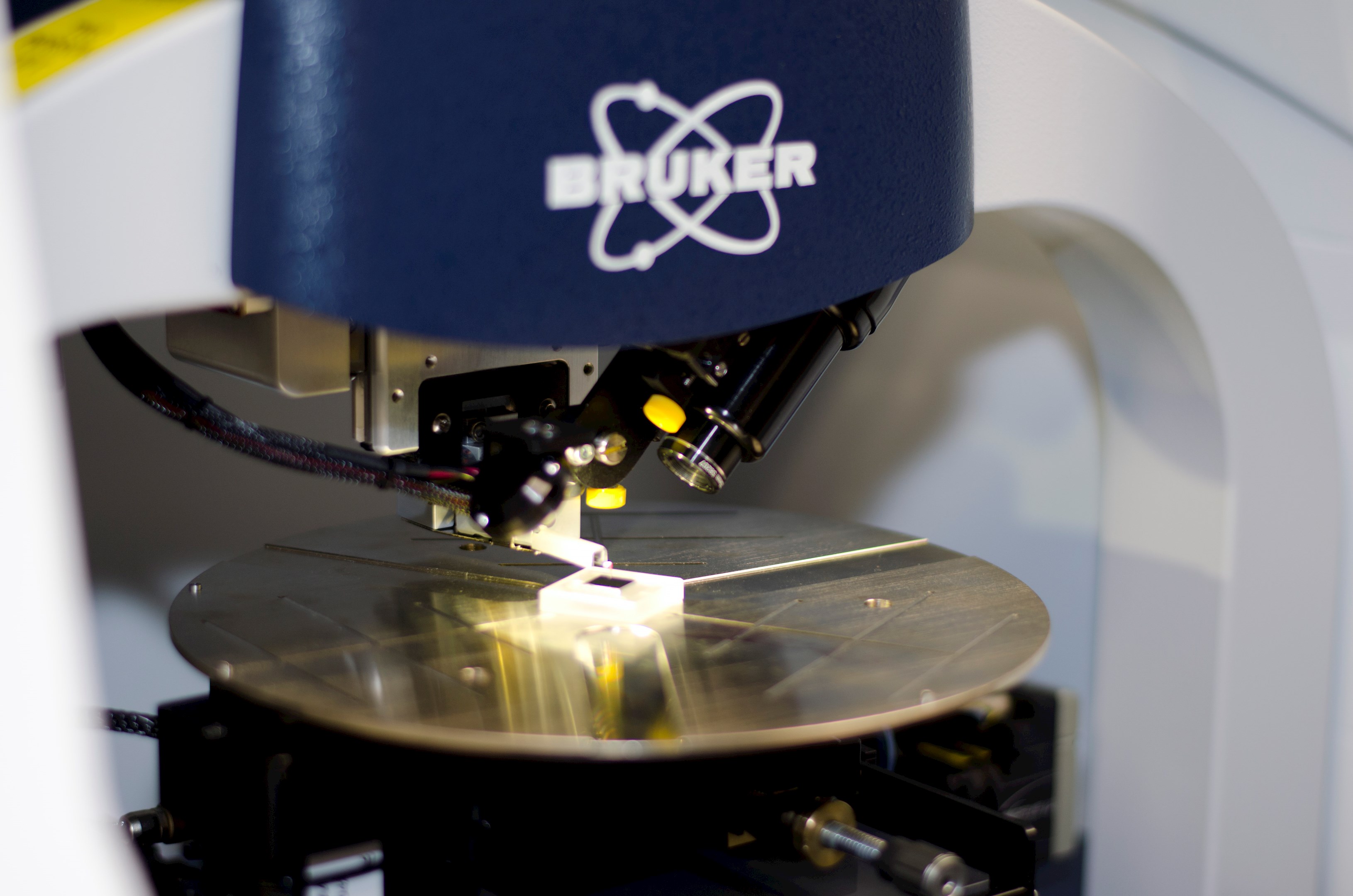
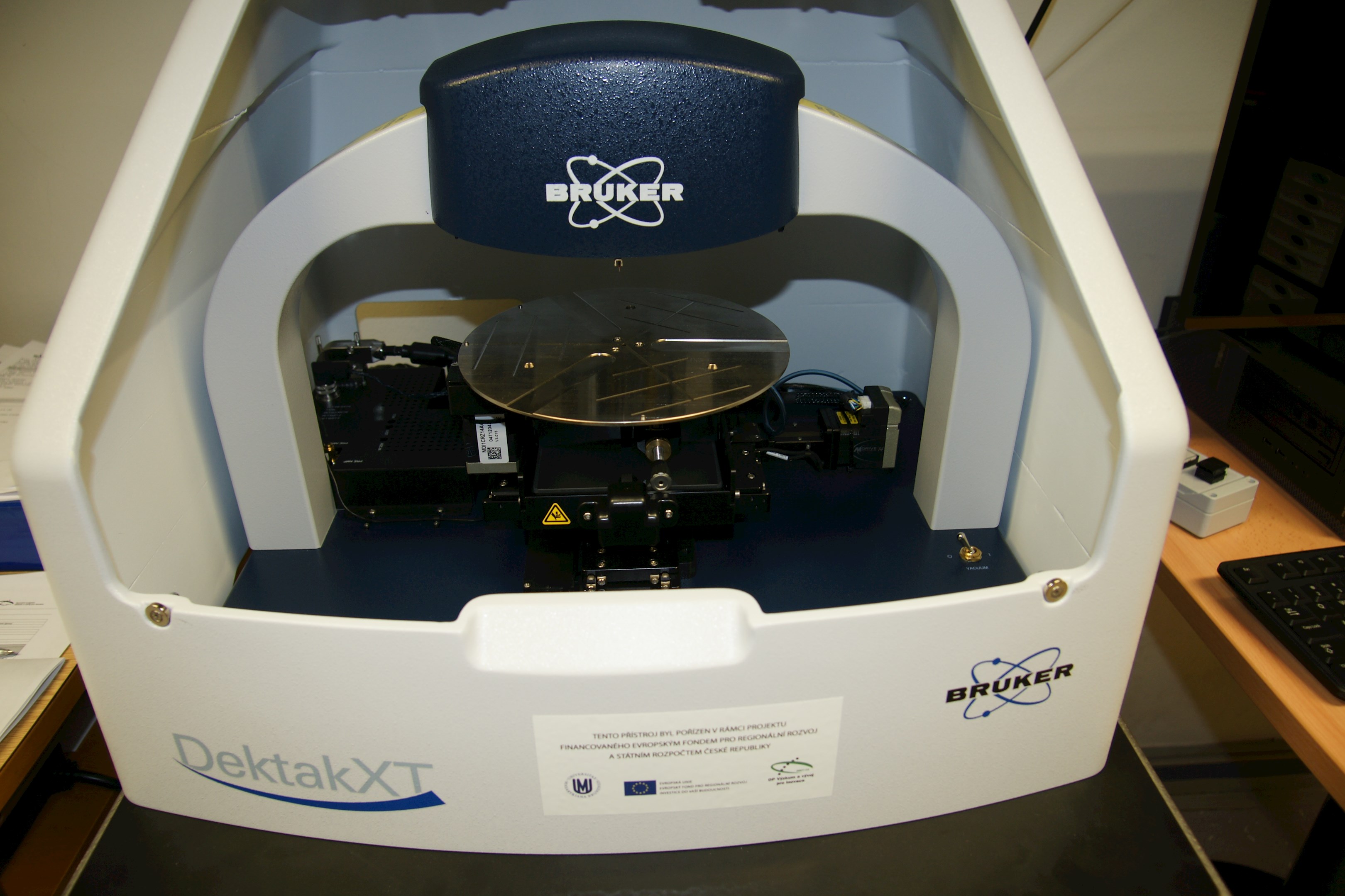
3D profilometer Bruker
The DektakXT stylus surface profiler is an advanced thin and thick film step height measurement tool.
Parameters:
- Measurement technique: Stylus profilometry (contact measurement)
- Measurement capability: Two-dimensional surface profile measurements Optional three-dimensional measurement/analyses
- Sample viewing: Digital magnification, 0.275 to 2.2mm vertical FOV
- Stylus sensor: Low Inertia Sensor (LIS 3)
- Stylus force: 1 to 15mg with LIS 3 sensor
- Low force option: N-Lite+ Low Force with 0.03 to 15mg (optional)
- Stylus options: Stylus radius options from 50nm to 25 m High Aspect Ratio (HAR) tips 10 m x 2 m and 200 m x 20 m; Custom tips available upon request
- Sample X/Y stage: Manual 100mm (4 in.) X/Y, manual leveling; Motorized 150mm (6 in.) X/Y, manual leveling
- Sample R-Theta stage: Manual, continuous 360 degrees; Motorized, continuous 360 degrees
- Scan length range: 55mm (2in.); 200mm (8in.) with scan stitching capability
- Data points per scan: 120000 maximum
- Max. sample thickness: 50mm (1.95in.)
- Max. wafer size: 200mm (8in.)
- Step height repeatability: <5Å, 1sigma on 0.1μm step
- Vertical range: 1mm (0.039in.)
- Vertical resolution: 1Å max. (@ 6.55_m range)
- Input power 100 – 240 VAC, 50 – 60Hz
- Temperature operating range: 20 to 25°C (68 to 77°F)
Scratch tester REVETEST Xpress plus CRM Instruments

The tester of adhesion REVETEST Xpress plus CRM Instruments is instrumentation for characterization of thin film-substrate systems (adhesion, fracture and deformation) and for quantification of coatings adhesion. The system includes penetration depth measurement, handling of large samples (up to 300 mm), video microscope for observation of failure creation, automatic software for adhesion and friction evaluation, real time display of normal force, friction force, friction coefficient, depth. The scratch modes includes constant, progressive and incremental loads, matrix of scratch tests and multicycles for wear studies. The load range covers testing loads from 0,5 to 200 N.
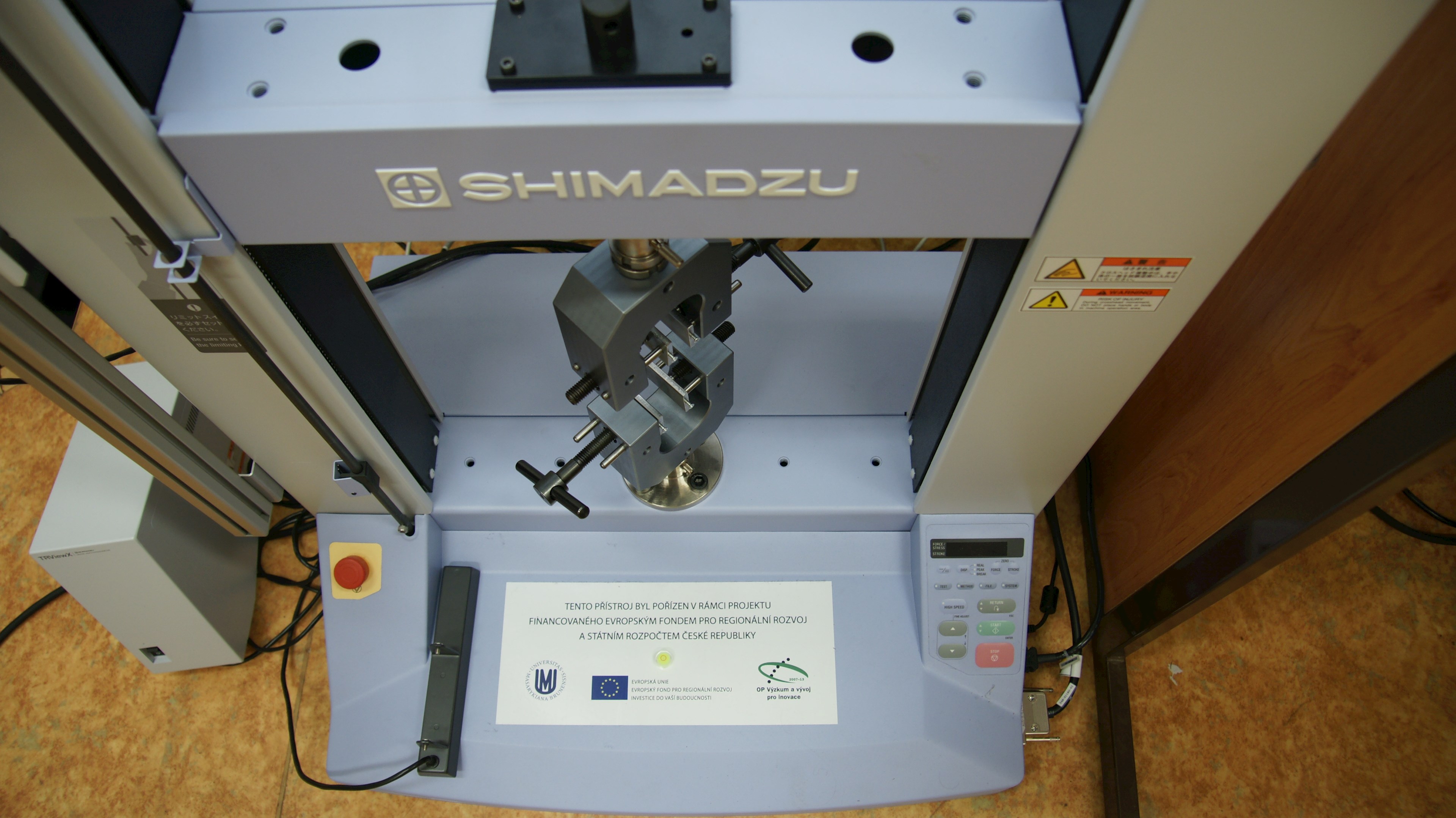
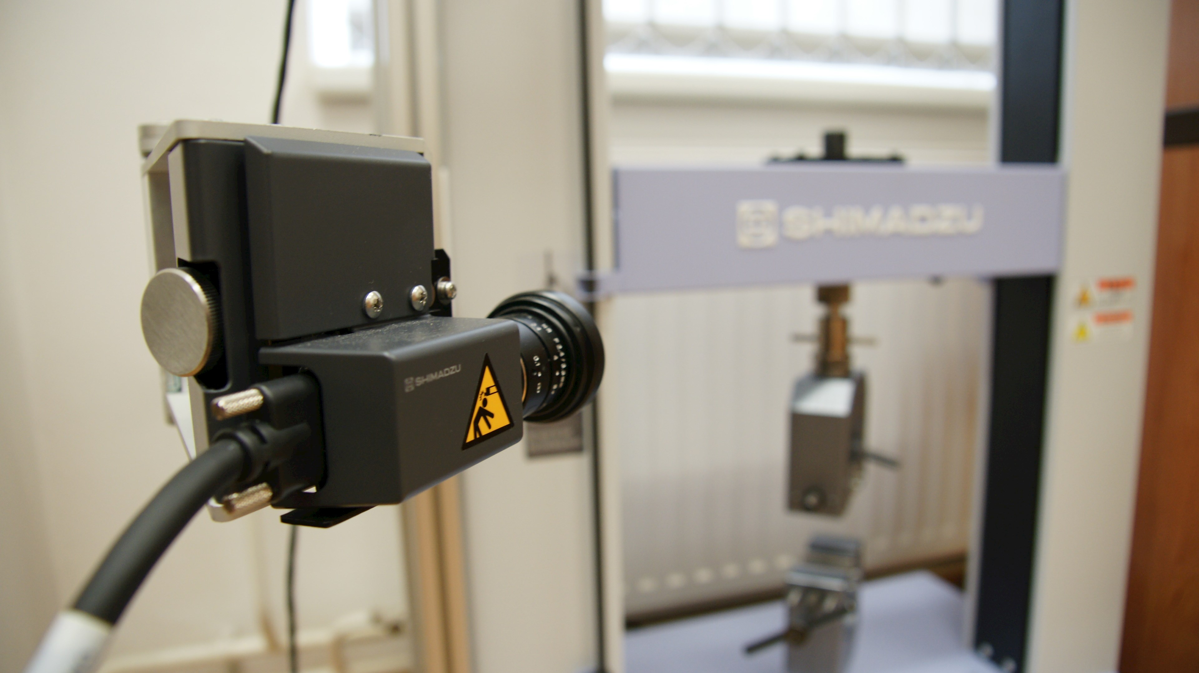
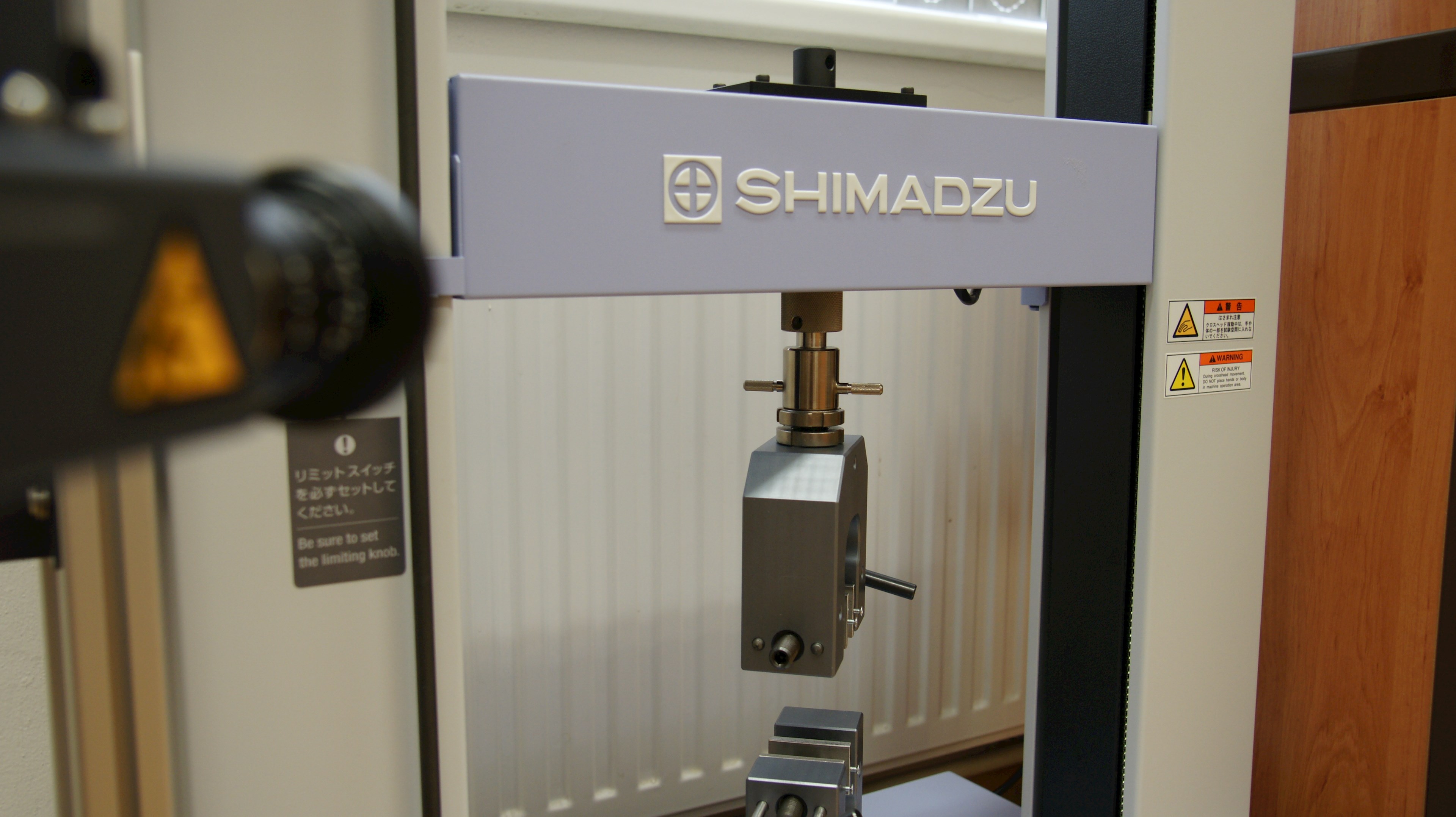
Tear machine Shimadzu
The tear machine AGS-5knX Shimadzu for defined straining of materials with automatic registration of the load and strain is intended to study the mechanical properties of materials. This equipment allows uniaxial tensile tests. The tear off testing is a programmable testing system.
Parameters:
- Force range: max 10kN, equipped by two dynamometer 100N and 5kN
- Loading method: Direct high-precision constant speed strain control method via non-backlash ball screw drive
- Force measurement: Within 1% indicated test force (at 1/500 to 1/1 load cell rating)
- Crosshead speed range: 0.001 to 1000 mm/min (stepless)

Are you interested to use our equipment? Contact us.
We send the cost and conditions of using our equipment on request.